

6.3
in intrinsic semiconductors the concentration of electrons is equal to the concentration of
holes. In intrinsic silicon at 300 K approximately 1.5 × 10
10
cm
−3 broken bonds are
present. This number then also gives the concentration of holes, p, and electrons, n.
Hence, at 300 K, n = p = 1.5 × 10
10
cm
−3
. This concentration is called the intrinsic carrier
concentration and is denoted as n i .
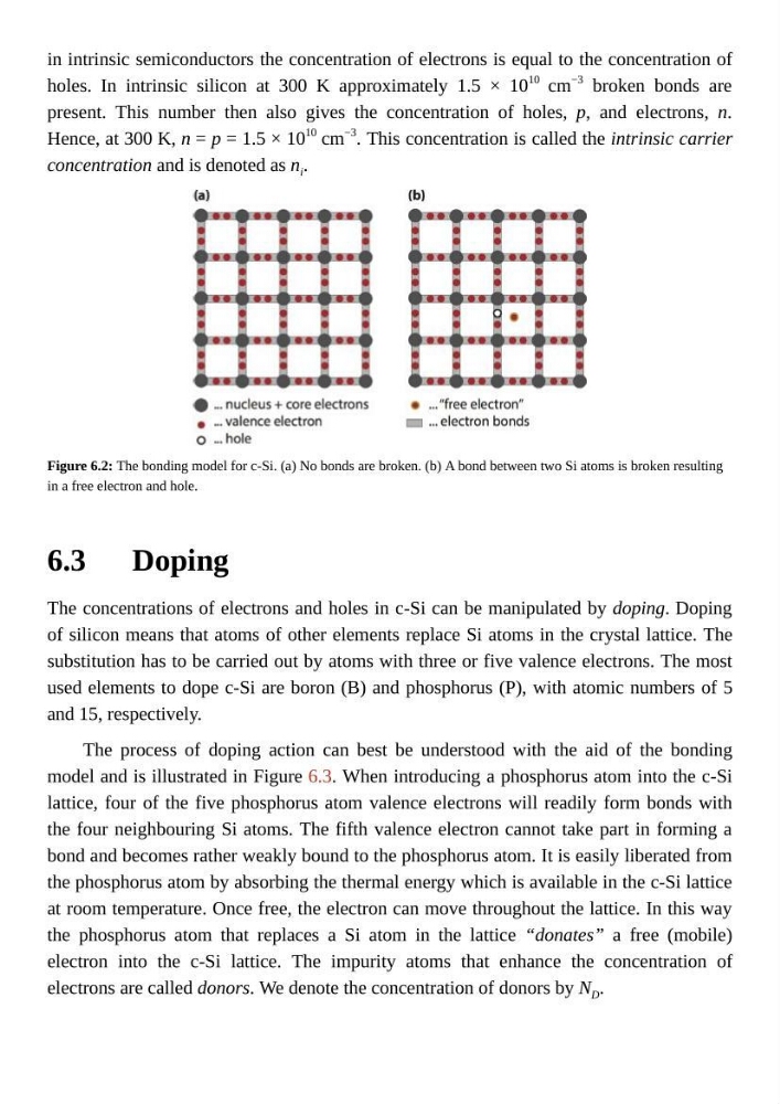
Figure 6.2: The bonding model for c-Si. (a) No bonds are broken. (b) A bond between two Si atoms is broken resulting
in a free electron and hole.
Doping
The concentrations of electrons and holes in c-Si can be manipulated by doping. Doping
of silicon means that atoms of other elements replace Si atoms in the crystal lattice. The
substitution has to be carried out by atoms with three or five valence electrons. The most
used elements to dope c-Si are boron (B) and phosphorus (P), with atomic numbers of 5
and 15, respectively.
The process of doping action can best be understood with the aid of the bonding
model and is illustrated in Figure 6.3. When introducing a phosphorus atom into the c-Si
lattice, four of the five phosphorus atom valence electrons will readily form bonds with
the four neighbouring Si atoms. The fifth valence electron cannot take part in forming a
bond and becomes rather weakly bound to the phosphorus atom. It is easily liberated from
the phosphorus atom by absorbing the thermal energy which is available in the c-Si lattice
at room temperature. Once free, the electron can move throughout the lattice. In this way
the phosphorus atom that replaces a Si atom in the lattice “donates” a free (mobile)
electron into the c-Si lattice. The impurity atoms that enhance the concentration of
electrons are called donors. We denote the concentration of donors by N D .
in intrinsic semiconductors the concentration of electrons is equal to the concentration of
holes. In intrinsic silicon at 300 K approximately 1.5 × 10
10
cm
−3 broken bonds are
present. This number then also gives the concentration of holes, p, and electrons, n.
Hence, at 300 K, n = p = 1.5 × 10
10
cm
−3
. This concentration is called the intrinsic carrier
concentration and is denoted as n i .
Figure 6.2: The bonding model for c-Si. (a) No bonds are broken. (b) A bond between two Si atoms is broken resulting
in a free electron and hole.
Doping
The concentrations of electrons and holes in c-Si can be manipulated by doping. Doping
of silicon means that atoms of other elements replace Si atoms in the crystal lattice. The
substitution has to be carried out by atoms with three or five valence electrons. The most
used elements to dope c-Si are boron (B) and phosphorus (P), with atomic numbers of 5
and 15, respectively.
The process of doping action can best be understood with the aid of the bonding
model and is illustrated in Figure 6.3. When introducing a phosphorus atom into the c-Si
lattice, four of the five phosphorus atom valence electrons will readily form bonds with
the four neighbouring Si atoms. The fifth valence electron cannot take part in forming a
bond and becomes rather weakly bound to the phosphorus atom. It is easily liberated from
the phosphorus atom by absorbing the thermal energy which is available in the c-Si lattice
at room temperature. Once free, the electron can move throughout the lattice. In this way
the phosphorus atom that replaces a Si atom in the lattice “donates” a free (mobile)
electron into the c-Si lattice. The impurity atoms that enhance the concentration of
electrons are called donors. We denote the concentration of donors by N D .