

1.
2.
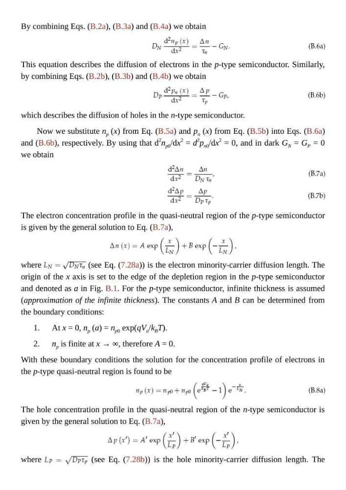
By combining Eqs. (B.2a), (B.3a) and (B.4a) we obtain
This equation describes the diffusion of electrons in the p-type semiconductor. Similarly,
by combining Eqs. (B.2b), (B.3b) and (B.4b) we obtain
which describes the diffusion of holes in the n-type semiconductor.
Now we substitute n p (x) from Eq. (B.5a) and p n (x) from Eq. (B.5b) into Eqs. (B.6a)
and (B.6b), respectively. By using that d
2
n p0 /dx
2 = d
2
p n0 /dx
2
= 0, and in dark G N = G P = 0
we obtain
The electron concentration profile in the quasi-neutral region of the p-type semiconductor
is given by the general solution to Eq. (B.7a),
where
(see Eq. (7.28a)) is the electron minority-carrier diffusion length. The
origin of the x axis is set to the edge of the depletion region in the p-type semiconductor
and denoted as a in Fig. B.1. For the p-type semiconductor, infinite thickness is assumed
(approximation of the infinite thickness). The constants A and B can be determined from
the boundary conditions:
At x = 0, n p (a) = n p0 exp(qV a /k B T).
n p is finite at x → ∞, therefore A = 0.
With these boundary conditions the solution for the concentration profile of electrons in
the p-type quasi-neutral region is found to be
The hole concentration profile in the quasi-neutral region of the n-type semiconductor is
given by the general solution to Eq. (B.7a),
where
(see Eq. (7.28b)) is the hole minority-carrier diffusion length. The
2.
By combining Eqs. (B.2a), (B.3a) and (B.4a) we obtain
This equation describes the diffusion of electrons in the p-type semiconductor. Similarly,
by combining Eqs. (B.2b), (B.3b) and (B.4b) we obtain
which describes the diffusion of holes in the n-type semiconductor.
Now we substitute n p (x) from Eq. (B.5a) and p n (x) from Eq. (B.5b) into Eqs. (B.6a)
and (B.6b), respectively. By using that d
2
n p0 /dx
2 = d
2
p n0 /dx
2
= 0, and in dark G N = G P = 0
we obtain
The electron concentration profile in the quasi-neutral region of the p-type semiconductor
is given by the general solution to Eq. (B.7a),
where
(see Eq. (7.28a)) is the electron minority-carrier diffusion length. The
origin of the x axis is set to the edge of the depletion region in the p-type semiconductor
and denoted as a in Fig. B.1. For the p-type semiconductor, infinite thickness is assumed
(approximation of the infinite thickness). The constants A and B can be determined from
the boundary conditions:
At x = 0, n p (a) = n p0 exp(qV a /k B T).
n p is finite at x → ∞, therefore A = 0.
With these boundary conditions the solution for the concentration profile of electrons in
the p-type quasi-neutral region is found to be
The hole concentration profile in the quasi-neutral region of the n-type semiconductor is
given by the general solution to Eq. (B.7a),
where
(see Eq. (7.28b)) is the hole minority-carrier diffusion length. The