

the current and conduct it to the bottom of the module where they are connected with
external cables.
The series connection is established with laser scribing. In total, three laser scribes
are required for separating two cells from each other and establishing a series connection
between them. The first laser scribe, called P1, is performed after the transparent front
contact is deposited, as shown in Figure 15.6 (a). The wavelength of the laser is such that
the laser light is absorbed in the front contact and the material is evaporated, leaving a
‘gap’ in the front contact, as shown in Figure 15.6 (b). Then the photoactive layers are
deposited onto the front contact and also fill the gaps. Then, the second laser scribe, called
P2, is performed, as illustrated in Figure 15.6 (c). The laser wavelength has to be chosen
such that it is not absorbed in the transparent front contact but in the absorber layer. For
example, if the absorber consists of amorphous silicon, green laser light can be used. The
P2 scribe leaves a gap in the absorber layer, as illustrated in Figure 15.6 (d). The next step
is the deposition of the metallic back contact that also fills the P2 gap. Finally, the third
laser scribe (P3) is performed as illustrated in Figure 15.6 (e). The wavelength for this
scribe has to be chosen such that it is neither absorbed in the front contact nor in the
absorber stack, so it maybe, for example, infrared. The P3 scribe shoots a gap into the
back contact, as shown in Figure 15.6 (f).
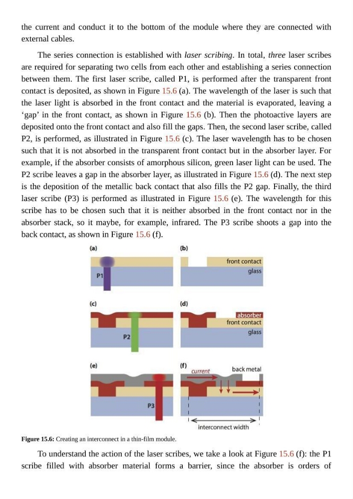
Figure 15.6: Creating an interconnect in a thin-film module.
To understand the action of the laser scribes, we take a look at Figure 15.6 (f): the P1
scribe filled with absorber material forms a barrier, since the absorber is orders of
external cables.
The series connection is established with laser scribing. In total, three laser scribes
are required for separating two cells from each other and establishing a series connection
between them. The first laser scribe, called P1, is performed after the transparent front
contact is deposited, as shown in Figure 15.6 (a). The wavelength of the laser is such that
the laser light is absorbed in the front contact and the material is evaporated, leaving a
‘gap’ in the front contact, as shown in Figure 15.6 (b). Then the photoactive layers are
deposited onto the front contact and also fill the gaps. Then, the second laser scribe, called
P2, is performed, as illustrated in Figure 15.6 (c). The laser wavelength has to be chosen
such that it is not absorbed in the transparent front contact but in the absorber layer. For
example, if the absorber consists of amorphous silicon, green laser light can be used. The
P2 scribe leaves a gap in the absorber layer, as illustrated in Figure 15.6 (d). The next step
is the deposition of the metallic back contact that also fills the P2 gap. Finally, the third
laser scribe (P3) is performed as illustrated in Figure 15.6 (e). The wavelength for this
scribe has to be chosen such that it is neither absorbed in the front contact nor in the
absorber stack, so it maybe, for example, infrared. The P3 scribe shoots a gap into the
back contact, as shown in Figure 15.6 (f).
Figure 15.6: Creating an interconnect in a thin-film module.
To understand the action of the laser scribes, we take a look at Figure 15.6 (f): the P1
scribe filled with absorber material forms a barrier, since the absorber is orders of