

achieved in single-junction amorphous silicon solar cells are 17 up to 18 mAcm
−2
, whereas
the maximum theoretic current that could be achieved up to 700 nm is in the order of 23
mAcm
−2
. Thus, the EQE averaged over the spectrum is in the order of 74 to 77%.
The highest achieved open circuit voltages are in the order of 1.0 V. With respect to a
bandgap of 1.75 eV, the bandgap utilization is quite low because of the high levels of
Shockley–Read–Hall recombination and the relatively broad valence and conduction-band
tails. The highest stabilized efficiency of single junction solar cells is 10.1% [47]. It was
obtained by the research Oerlikon Solar Lab in Switzerland, which is currently a
subsidiary of the Japanese Tokyo Electron Ltd.
Besides a-Si:H, nanocrystalline silicon films are also used for the intrinsic absorber
layers in p-i-n solar cells as well. The spectral utilization of the nc-Si:H is better than that
of amorphous silicon because of the lower bandgap of nc-Si:H. However, to utilize the
spectral part from 700 up to 950 nm, thicker films are required, because of the indirect
bandgap of the silicon crystallites. Typical intrinsic film thicknesses are between 1 μm and
3 μm. The current nc-Si:H record cell has a short circuit current density of 28.8 mAcm
−2
,
an open circuit voltage of 523 mV and an efficiency of 10.8% [47]. This result was
achieved by the Japanese Institute of Advanced Industrial Science and Technology
(AIST).
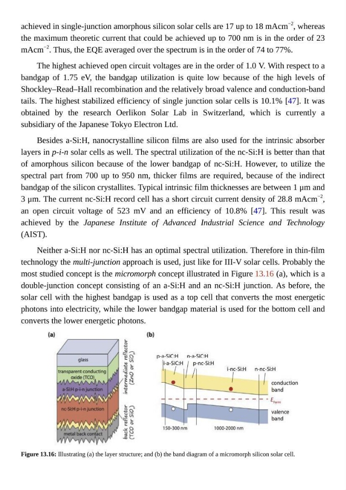
Neither a-Si:H nor nc-Si:H has an optimal spectral utilization. Therefore in thin-film
technology the multi-junction approach is used, just like for III-V solar cells. Probably the
most studied concept is the micromorph concept illustrated in Figure 13.16 (a), which is a
double-junction concept consisting of an a-Si:H and an nc-Si:H junction. As before, the
solar cell with the highest bandgap is used as a top cell that converts the most energetic
photons into electricity, while the lower bandgap material is used for the bottom cell and
converts the lower energetic photons.
Figure 13.16: Illustrating (a) the layer structure; and (b) the band diagram of a micromorph silicon solar cell.
−2
, whereas
the maximum theoretic current that could be achieved up to 700 nm is in the order of 23
mAcm
−2
. Thus, the EQE averaged over the spectrum is in the order of 74 to 77%.
The highest achieved open circuit voltages are in the order of 1.0 V. With respect to a
bandgap of 1.75 eV, the bandgap utilization is quite low because of the high levels of
Shockley–Read–Hall recombination and the relatively broad valence and conduction-band
tails. The highest stabilized efficiency of single junction solar cells is 10.1% [47]. It was
obtained by the research Oerlikon Solar Lab in Switzerland, which is currently a
subsidiary of the Japanese Tokyo Electron Ltd.
Besides a-Si:H, nanocrystalline silicon films are also used for the intrinsic absorber
layers in p-i-n solar cells as well. The spectral utilization of the nc-Si:H is better than that
of amorphous silicon because of the lower bandgap of nc-Si:H. However, to utilize the
spectral part from 700 up to 950 nm, thicker films are required, because of the indirect
bandgap of the silicon crystallites. Typical intrinsic film thicknesses are between 1 μm and
3 μm. The current nc-Si:H record cell has a short circuit current density of 28.8 mAcm
−2
,
an open circuit voltage of 523 mV and an efficiency of 10.8% [47]. This result was
achieved by the Japanese Institute of Advanced Industrial Science and Technology
(AIST).
Neither a-Si:H nor nc-Si:H has an optimal spectral utilization. Therefore in thin-film
technology the multi-junction approach is used, just like for III-V solar cells. Probably the
most studied concept is the micromorph concept illustrated in Figure 13.16 (a), which is a
double-junction concept consisting of an a-Si:H and an nc-Si:H junction. As before, the
solar cell with the highest bandgap is used as a top cell that converts the most energetic
photons into electricity, while the lower bandgap material is used for the bottom cell and
converts the lower energetic photons.
Figure 13.16: Illustrating (a) the layer structure; and (b) the band diagram of a micromorph silicon solar cell.