

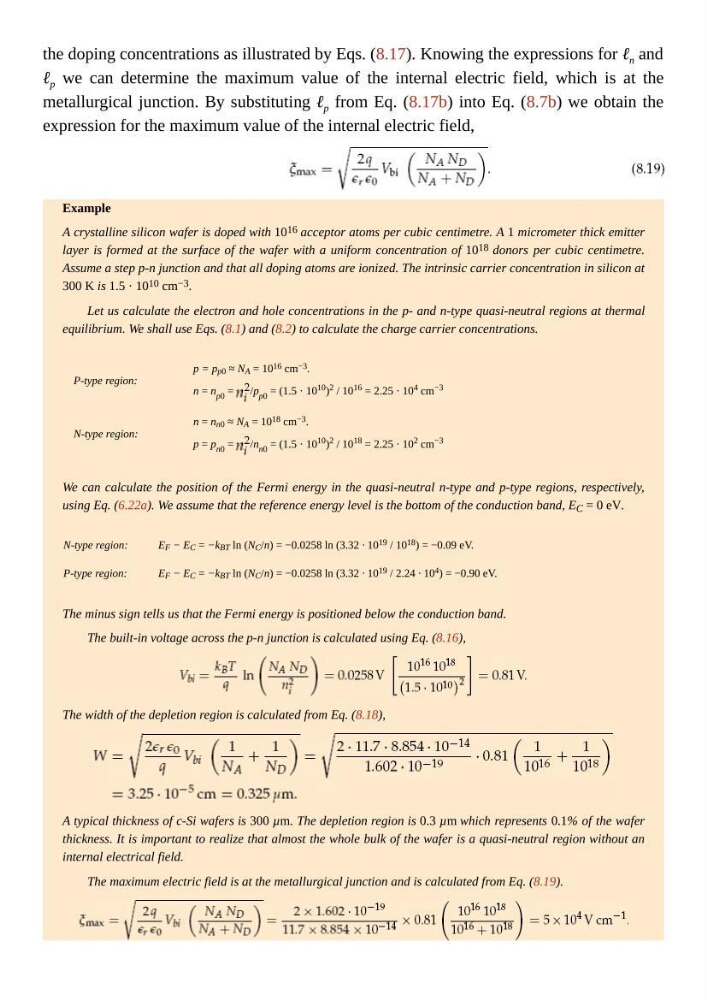
the doping concentrations as illustrated by Eqs. (8.17). Knowing the expressions for ℓ n and
ℓ p we can determine the maximum value of the internal electric field, which is at the
metallurgical junction. By substituting ℓ p from Eq. (8.17b) into Eq. (8.7b) we obtain the
expression for the maximum value of the internal electric field,
Example
A crystalline silicon wafer is doped with 10 16 acceptor atoms per cubic centimetre. A 1 micrometer thick emitter
layer is formed at the surface of the wafer with a uniform concentration of 10 18 donors per cubic centimetre.
Assume a step p-n junction and that all doping atoms are ionized. The intrinsic carrier concentration in silicon at
300 K is 1.5 · 10 10 cm −3 .
Let us calculate the electron and hole concentrations in the p- and n-type quasi-neutral regions at thermal
equilibrium. We shall use Eqs. (8.1) and (8.2) to calculate the charge carrier concentrations.
P-type region:
p = p p0 ≈ N A = 10 16 cm −3 .
n = n p0 = /p p0 = (1.5 · 10 10 ) 2 / 10 16 = 2.25 · 10 4 cm −3
N-type region:
n = n n0 ≈ N A = 10 18 cm −3 .
p = p n0 = /n n0 = (1.5 · 10 10 ) 2 / 10 18 = 2.25 · 10 2 cm −3
We can calculate the position of the Fermi energy in the quasi-neutral n-type and p-type regions, respectively,
using Eq. (6.22a). We assume that the reference energy level is the bottom of the conduction band, E C = 0 eV.
N-type region:
E F − E C = −k BT ln (N C /n) = −0.0258 ln (3.32 · 10 19 / 10 18 ) = −0.09 eV.
P-type region:
E F − E C = −k BT ln (N C /n) = −0.0258 ln (3.32 · 10 19 / 2.24 · 10 4 ) = −0.90 eV.
The minus sign tells us that the Fermi energy is positioned below the conduction band.
The built-in voltage across the p-n junction is calculated using Eq. (8.16),
The width of the depletion region is calculated from Eq. (8.18),
A typical thickness of c-Si wafers is 300 µm. The depletion region is 0.3 µm which represents 0.1% of the wafer
thickness. It is important to realize that almost the whole bulk of the wafer is a quasi-neutral region without an
internal electrical field.
The maximum electric field is at the metallurgical junction and is calculated from Eq. (8.19).
ℓ p we can determine the maximum value of the internal electric field, which is at the
metallurgical junction. By substituting ℓ p from Eq. (8.17b) into Eq. (8.7b) we obtain the
expression for the maximum value of the internal electric field,
Example
A crystalline silicon wafer is doped with 10 16 acceptor atoms per cubic centimetre. A 1 micrometer thick emitter
layer is formed at the surface of the wafer with a uniform concentration of 10 18 donors per cubic centimetre.
Assume a step p-n junction and that all doping atoms are ionized. The intrinsic carrier concentration in silicon at
300 K is 1.5 · 10 10 cm −3 .
Let us calculate the electron and hole concentrations in the p- and n-type quasi-neutral regions at thermal
equilibrium. We shall use Eqs. (8.1) and (8.2) to calculate the charge carrier concentrations.
P-type region:
p = p p0 ≈ N A = 10 16 cm −3 .
n = n p0 = /p p0 = (1.5 · 10 10 ) 2 / 10 16 = 2.25 · 10 4 cm −3
N-type region:
n = n n0 ≈ N A = 10 18 cm −3 .
p = p n0 = /n n0 = (1.5 · 10 10 ) 2 / 10 18 = 2.25 · 10 2 cm −3
We can calculate the position of the Fermi energy in the quasi-neutral n-type and p-type regions, respectively,
using Eq. (6.22a). We assume that the reference energy level is the bottom of the conduction band, E C = 0 eV.
N-type region:
E F − E C = −k BT ln (N C /n) = −0.0258 ln (3.32 · 10 19 / 10 18 ) = −0.09 eV.
P-type region:
E F − E C = −k BT ln (N C /n) = −0.0258 ln (3.32 · 10 19 / 2.24 · 10 4 ) = −0.90 eV.
The minus sign tells us that the Fermi energy is positioned below the conduction band.
The built-in voltage across the p-n junction is calculated using Eq. (8.16),
The width of the depletion region is calculated from Eq. (8.18),
A typical thickness of c-Si wafers is 300 µm. The depletion region is 0.3 µm which represents 0.1% of the wafer
thickness. It is important to realize that almost the whole bulk of the wafer is a quasi-neutral region without an
internal electrical field.
The maximum electric field is at the metallurgical junction and is calculated from Eq. (8.19).