

177
Noise in Strain-Engineered Devices
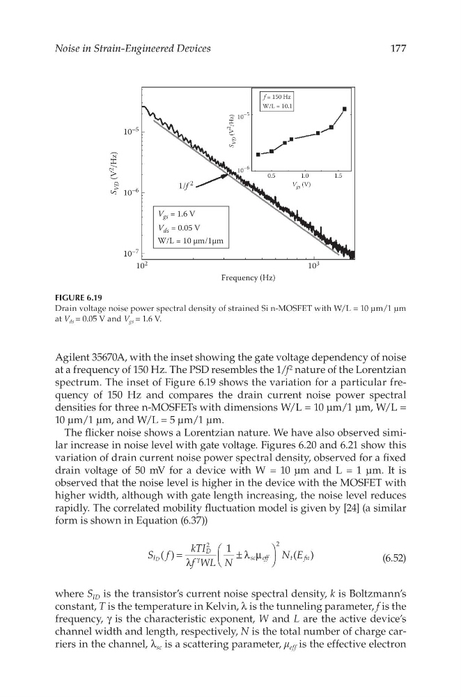
Agilent 35670A, with the inset showing the gate voltage dependency of noise
at a frequency of 150 Hz. The PSD resembles the 1/f 2 nature of the Lorentzian
spectrum. The inset of Figure 6.19 shows the variation for a particular frequency of 150 Hz and compares the drain current noise power spectral
densities for three n-MOSFETs with dimensions W/L = 10 µm/1 µm, W/L =
10 µm/1 µm, and W/L = 5 µm/1 µm.
The flicker noise shows a Lorentzian nature. We have also observed similar increase in noise level with gate voltage. Figures 6.20 and 6.21 show this
variation of drain current noise power spectral density, observed for a fixed
drain voltage of 50 mV for a device with W = 10 µm and L = 1 µm. It is
observed that the noise level is higher in the device with the MOSFET with
higher width, although with gate length increasing, the noise level reduces
rapidly. The correlated mobility fluctuation model is given by [24] (a similar
form is shown in Equation (6.37))
S f
kTI
f WL N
N E
( )
1
( )
I
D
sc eff
t
fn
2
2
D
= λ
± λ µ
γ
(6.52)
where S ID is the transistor’s current noise spectral density, k is Boltzmann’s
constant, T is the temperature in Kelvin, λ is the tunneling parameter, f is the
frequency, γ is the characteristic exponent, W and L are the active device’s
channel width and length, respectively, N is the total number of charge carriers in the channel, λ sc is a scattering parameter, μ eff is the effective electron
10
–5
10
–6
10
–7
1.5
1.0
10
–6
10
–5
0.5
V gs (V)
f = 150 Hz
W/L = 10.1
10
2
10
3
S
VD (V
2
/Hz)
S
VD (V
2
/Hz)
V gs = 1.6 V
V ds = 0.05 V
W/L = 10 µm/1µm
Frequency (Hz)
1/f
2
FIGURE 6.19
Drain voltage noise power spectral density of strained Si n-MOSFET with W/L = 10 µm/1 µm
at V ds = 0.05 V and V gs = 1.6 V.
Noise in Strain-Engineered Devices
Agilent 35670A, with the inset showing the gate voltage dependency of noise
at a frequency of 150 Hz. The PSD resembles the 1/f 2 nature of the Lorentzian
spectrum. The inset of Figure 6.19 shows the variation for a particular frequency of 150 Hz and compares the drain current noise power spectral
densities for three n-MOSFETs with dimensions W/L = 10 µm/1 µm, W/L =
10 µm/1 µm, and W/L = 5 µm/1 µm.
The flicker noise shows a Lorentzian nature. We have also observed similar increase in noise level with gate voltage. Figures 6.20 and 6.21 show this
variation of drain current noise power spectral density, observed for a fixed
drain voltage of 50 mV for a device with W = 10 µm and L = 1 µm. It is
observed that the noise level is higher in the device with the MOSFET with
higher width, although with gate length increasing, the noise level reduces
rapidly. The correlated mobility fluctuation model is given by [24] (a similar
form is shown in Equation (6.37))
S f
kTI
f WL N
N E
( )
1
( )
I
D
sc eff
t
fn
2
2
D
= λ
± λ µ
γ
(6.52)
where S ID is the transistor’s current noise spectral density, k is Boltzmann’s
constant, T is the temperature in Kelvin, λ is the tunneling parameter, f is the
frequency, γ is the characteristic exponent, W and L are the active device’s
channel width and length, respectively, N is the total number of charge carriers in the channel, λ sc is a scattering parameter, μ eff is the effective electron
10
–5
10
–6
10
–7
1.5
1.0
10
–6
10
–5
0.5
V gs (V)
f = 150 Hz
W/L = 10.1
10
2
10
3
S
VD (V
2
/Hz)
S
VD (V
2
/Hz)
V gs = 1.6 V
V ds = 0.05 V
W/L = 10 µm/1µm
Frequency (Hz)
1/f
2
FIGURE 6.19
Drain voltage noise power spectral density of strained Si n-MOSFET with W/L = 10 µm/1 µm
at V ds = 0.05 V and V gs = 1.6 V.