

165
Noise in Strain-Engineered Devices
that Equation (6.38) holds, the PSD can be expressed as a linear function of
frequency on a log-log plot,
S f
S
Hz
f
log[ ( )] log[ (1 )]
log[ ]
I
I
D
D
=
− γ
(6.39)
Although the PSD data follow 1/f γ dependence over a wide frequency range,
Equation (6.38) applies only for a smaller range of frequencies locally, and
the noise exponent, γ, and the magnitude, S ID (1 Hz), are frequency independent. But both the noise exponent and the magnitude are affected by
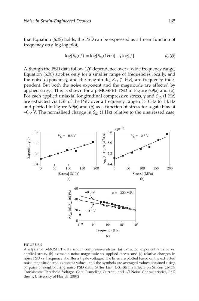
applied stress. This is shown for a p-MOSFET PSD in Figure 6.9(a) and (b).
For each applied uniaxial longitudinal compressive stress, γ and S ID (1 Hz)
are extracted via LSF of the PSD over a frequency range of 30 Hz to 1 kHz
and plotted in Figure 6.9(a) and (b) as a function of stress for a gate bias of
–0.6 V. The normalised change in S ID (1 Hz) relative to the unstressed case,
1.07
1.06
Exponent γ(σ)
σ = –200 MPa
–0.8 V
–0.6 V
1.05
1.04
0
5 0
100
V G = –0.6 V
|Stress| (MPa)
(a)
150
200
6.8
×10
–13
6.0
S
ID (1 Hz, σ) (A
2
/Hz)
5.2
4.4
0
5 0
100
V G = –0.6 V
|Stress| (MPa)
(b)
150
200
60
40
∆S
ID (σ)/S
ID (0) (%)
20
0
10
0
10
1
10
2
Frequency (Hz)
(c)
10
3
10
4
FIGURE 6.9
Analysis of p-MOSFET data under compressive stress: (a) extracted exponent γ value vs.
applied stress, (b) extracted noise magnitude vs. applied stress, and (c) relative changes in
noise PSD vs. frequency at different gate voltages. The lines are plotted based on the extracted
noise magnitude and exponent values, and the symbols are averaged values obtained using
50 pairs of neighbouring noise PSD data. (After Lim, J.-S., Strain Effects on Silicon CMOS
Transistors: Threshold Voltage, Gate Tunneling Current, and 1/f Noise Characteristics, PhD
thesis, University of Florida, 2007.)
Noise in Strain-Engineered Devices
that Equation (6.38) holds, the PSD can be expressed as a linear function of
frequency on a log-log plot,
S f
S
Hz
f
log[ ( )] log[ (1 )]
log[ ]
I
I
D
D
=
− γ
(6.39)
Although the PSD data follow 1/f γ dependence over a wide frequency range,
Equation (6.38) applies only for a smaller range of frequencies locally, and
the noise exponent, γ, and the magnitude, S ID (1 Hz), are frequency independent. But both the noise exponent and the magnitude are affected by
applied stress. This is shown for a p-MOSFET PSD in Figure 6.9(a) and (b).
For each applied uniaxial longitudinal compressive stress, γ and S ID (1 Hz)
are extracted via LSF of the PSD over a frequency range of 30 Hz to 1 kHz
and plotted in Figure 6.9(a) and (b) as a function of stress for a gate bias of
–0.6 V. The normalised change in S ID (1 Hz) relative to the unstressed case,
1.07
1.06
Exponent γ(σ)
σ = –200 MPa
–0.8 V
–0.6 V
1.05
1.04
0
5 0
100
V G = –0.6 V
|Stress| (MPa)
(a)
150
200
6.8
×10
–13
6.0
S
ID (1 Hz, σ) (A
2
/Hz)
5.2
4.4
0
5 0
100
V G = –0.6 V
|Stress| (MPa)
(b)
150
200
60
40
∆S
ID (σ)/S
ID (0) (%)
20
0
10
0
10
1
10
2
Frequency (Hz)
(c)
10
3
10
4
FIGURE 6.9
Analysis of p-MOSFET data under compressive stress: (a) extracted exponent γ value vs.
applied stress, (b) extracted noise magnitude vs. applied stress, and (c) relative changes in
noise PSD vs. frequency at different gate voltages. The lines are plotted based on the extracted
noise magnitude and exponent values, and the symbols are averaged values obtained using
50 pairs of neighbouring noise PSD data. (After Lim, J.-S., Strain Effects on Silicon CMOS
Transistors: Threshold Voltage, Gate Tunneling Current, and 1/f Noise Characteristics, PhD
thesis, University of Florida, 2007.)