

155
Noise in Strain-Engineered Devices
The fluctuation in the drain current I D = f(V fb , μ eff ) then yields [23]
I
I
V
V
I
Q
Q
or I
g V
I
Q
Q
,
D
D
fb
fb
D
eff
eff
ox
ox
D
m
fb
D
eff
eff
ox
ox
δ =
∂
∂
δ +
∂
∂µ
∂µ
∂
δ
δ = − δ + µ
∂µ
∂
δ
(6.18)
With
Q
1
eff
eff
ox
2
α = µ
∂µ
∂
(for n-MOSFET),
I
g V
I
C V
D
m
fb
D eff
ox
fb
δ = − δ − µ α δ
(6.19)
So, transferring Equation (6.19) into frequency domain, current noise power
spectral density becomes
S
S
C I
g
g
1
I
V
eff ox D
m
m
2
2
D
f b
=
+
αµ
(6.20)
The first term in the parentheses in Equation (6.20) is due to the fluctuating
number of inversion carriers, and the second term to mobility fluctuations
correlated to the number fluctuations. Note that α can be negative or positive
depending on if the mobility increases or decreases upon trapping a charge
according to Equation (6.18). The power spectral density of the flat-band
G
Gate oxide
Si p-type
n+
n+
S
D
–
–
–
–
–
–
–
–
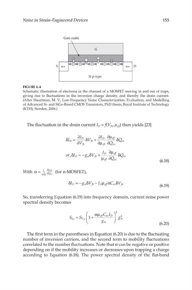
FIGURE 6.4
Schematic illustration of electrons in the channel of a MOSFET moving in and out of traps,
giving rise to fluctuations in the inversion charge density, and thereby the drain current.
(After Haartman, M. V., Low-Frequency Noise Characterization, Evaluation, and Modelling
of Advanced Si- and SiGe-Based CMOS Transistors, PhD thesis, Royal Institute of Technology
(KTH), Sweden, 2006.)
Noise in Strain-Engineered Devices
The fluctuation in the drain current I D = f(V fb , μ eff ) then yields [23]
I
I
V
V
I
Q
Q
or I
g V
I
Q
Q
,
D
D
fb
fb
D
eff
eff
ox
ox
D
m
fb
D
eff
eff
ox
ox
δ =
∂
∂
δ +
∂
∂µ
∂µ
∂
δ
δ = − δ + µ
∂µ
∂
δ
(6.18)
With
Q
1
eff
eff
ox
2
α = µ
∂µ
∂
(for n-MOSFET),
I
g V
I
C V
D
m
fb
D eff
ox
fb
δ = − δ − µ α δ
(6.19)
So, transferring Equation (6.19) into frequency domain, current noise power
spectral density becomes
S
S
C I
g
g
1
I
V
eff ox D
m
m
2
2
D
f b
=
+
αµ
(6.20)
The first term in the parentheses in Equation (6.20) is due to the fluctuating
number of inversion carriers, and the second term to mobility fluctuations
correlated to the number fluctuations. Note that α can be negative or positive
depending on if the mobility increases or decreases upon trapping a charge
according to Equation (6.18). The power spectral density of the flat-band
G
Gate oxide
Si p-type
n+
n+
S
D
–
–
–
–
–
–
–
–
FIGURE 6.4
Schematic illustration of electrons in the channel of a MOSFET moving in and out of traps,
giving rise to fluctuations in the inversion charge density, and thereby the drain current.
(After Haartman, M. V., Low-Frequency Noise Characterization, Evaluation, and Modelling
of Advanced Si- and SiGe-Based CMOS Transistors, PhD thesis, Royal Institute of Technology
(KTH), Sweden, 2006.)