

96
Strain-Engineered MOSFETs
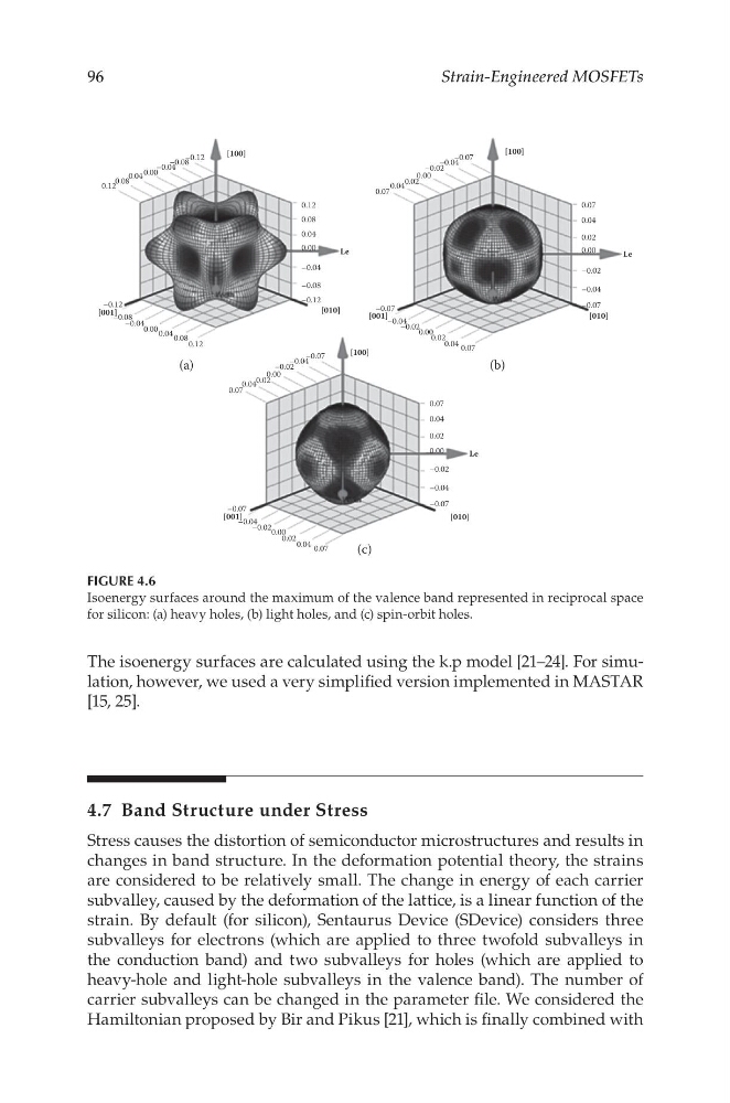
The isoenergy surfaces are calculated using the k.p model [21–24]. For simulation, however, we used a very simplified version implemented in MASTAR
[15, 25].
4.7 Band Structure under Stress
Stress causes the distortion of semiconductor microstructures and results in
changes in band structure. In the deformation potential theory, the strains
are considered to be relatively small. The change in energy of each carrier
subvalley, caused by the deformation of the lattice, is a linear function of the
strain. By default (for silicon), Sentaurus Device (SDevice) considers three
subvalleys for electrons (which are applied to three twofold subvalleys in
the conduction band) and two subvalleys for holes (which are applied to
heavy-hole and light-hole subvalleys in the valence band). The number of
carrier subvalleys can be changed in the parameter file. We considered the
Hamiltonian proposed by Bir and Pikus [21], which is finally combined with
0.12
0.12
0.12
–0.12
0.08
0.08
0.08
0.04
0.04
0.04
–0.04
–0.04
–0.04
–0.08
–0.07
–0.07
–0.07
–0.04
–0.04
–0.04
–0.02
–0.02
–0.02
0.02
0.02
0.02
0.04
0.04
0.04
0.07
0.07
0.07
0.00
0.00
–0.07
–0.04
–0.02
0.02 0.04 0.07
0.00
0.00
–0.07
–0.04
–0.02
0.02
0.04
0.07
0.00
–0.07
–0.04
–0.02
0.02
0.04
0.07
0.00
–0.08
–0.08
–0.12
–0.12
[100]
[100]
[100]
Le
Le
[001]
[001]
[001]
[010]
[010]
(a)
(b)
(c)
[010]
Le
0.00
0.00
0.00
FIGURE 4.6
Isoenergy surfaces around the maximum of the valence band represented in reciprocal space
for silicon: (a) heavy holes, (b) light holes, and (c) spin-orbit holes.
Strain-Engineered MOSFETs
The isoenergy surfaces are calculated using the k.p model [21–24]. For simulation, however, we used a very simplified version implemented in MASTAR
[15, 25].
4.7 Band Structure under Stress
Stress causes the distortion of semiconductor microstructures and results in
changes in band structure. In the deformation potential theory, the strains
are considered to be relatively small. The change in energy of each carrier
subvalley, caused by the deformation of the lattice, is a linear function of the
strain. By default (for silicon), Sentaurus Device (SDevice) considers three
subvalleys for electrons (which are applied to three twofold subvalleys in
the conduction band) and two subvalleys for holes (which are applied to
heavy-hole and light-hole subvalleys in the valence band). The number of
carrier subvalleys can be changed in the parameter file. We considered the
Hamiltonian proposed by Bir and Pikus [21], which is finally combined with
0.12
0.12
0.12
–0.12
0.08
0.08
0.08
0.04
0.04
0.04
–0.04
–0.04
–0.04
–0.08
–0.07
–0.07
–0.07
–0.04
–0.04
–0.04
–0.02
–0.02
–0.02
0.02
0.02
0.02
0.04
0.04
0.04
0.07
0.07
0.07
0.00
0.00
–0.07
–0.04
–0.02
0.02 0.04 0.07
0.00
0.00
–0.07
–0.04
–0.02
0.02
0.04
0.07
0.00
–0.07
–0.04
–0.02
0.02
0.04
0.07
0.00
–0.08
–0.08
–0.12
–0.12
[100]
[100]
[100]
Le
Le
[001]
[001]
[001]
[010]
[010]
(a)
(b)
(c)
[010]
Le
0.00
0.00
0.00
FIGURE 4.6
Isoenergy surfaces around the maximum of the valence band represented in reciprocal space
for silicon: (a) heavy holes, (b) light holes, and (c) spin-orbit holes.