

large scales. Many of the studied metamaterials to date rely on top-down lithographic
approaches that require access to cost-intensive nanofabrication facilities, which in
turn make large-scale fabrication of 3D metamaterials prohibitive.
For fabricating photonic crystals and metamaterials, bottom-up BCP SA may
offer a promising low-cost alternative, in particular for the fabrication of 3D
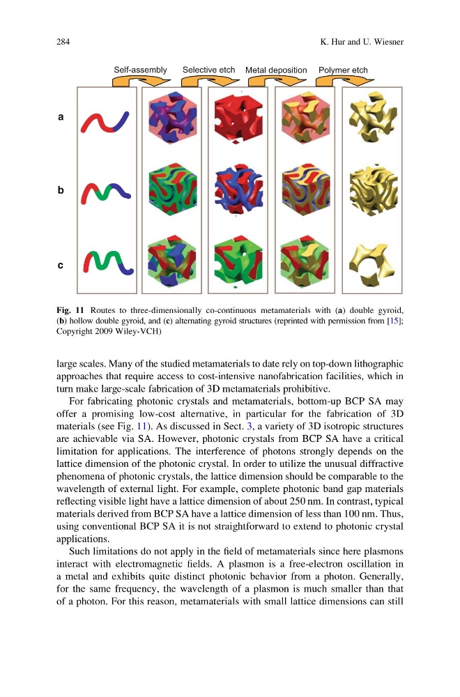
materials (see Fig. 11). As discussed in Sect. 3, a variety of 3D isotropic structures
are achievable via SA. However, photonic crystals from BCP SA have a critical
limitation for applications. The interference of photons strongly depends on the
lattice dimension of the photonic crystal. In order to utilize the unusual diffractive
phenomena of photonic crystals, the lattice dimension should be comparable to the
wavelength of external light. For example, complete photonic band gap materials
reflecting visible light have a lattice dimension of about 250 nm. In contrast, typical
materials derived from BCP SA have a lattice dimension of less than 100 nm. Thus,
using conventional BCP SA it is not straightforward to extend to photonic crystal
applications.
Such limitations do not apply in the field of metamaterials since here plasmons
interact with electromagnetic fields. A plasmon is a free-electron oscillation in
a metal and exhibits quite distinct photonic behavior from a photon. Generally,
for the same frequency, the wavelength of a plasmon is much smaller than that
of a photon. For this reason, metamaterials with small lattice dimensions can still
Self-assembly
Selective etch Metal deposition Polymer etch
a
b
c
Fig. 11 Routes to three-dimensionally co-continuous metamaterials with (a) double gyroid,
(b) hollow double gyroid, and (c) alternating gyroid structures (reprinted with permission from [15];
Copyright 2009 Wiley-VCH)
284
K. Hur and U. Wiesner
approaches that require access to cost-intensive nanofabrication facilities, which in
turn make large-scale fabrication of 3D metamaterials prohibitive.
For fabricating photonic crystals and metamaterials, bottom-up BCP SA may
offer a promising low-cost alternative, in particular for the fabrication of 3D
materials (see Fig. 11). As discussed in Sect. 3, a variety of 3D isotropic structures
are achievable via SA. However, photonic crystals from BCP SA have a critical
limitation for applications. The interference of photons strongly depends on the
lattice dimension of the photonic crystal. In order to utilize the unusual diffractive
phenomena of photonic crystals, the lattice dimension should be comparable to the
wavelength of external light. For example, complete photonic band gap materials
reflecting visible light have a lattice dimension of about 250 nm. In contrast, typical
materials derived from BCP SA have a lattice dimension of less than 100 nm. Thus,
using conventional BCP SA it is not straightforward to extend to photonic crystal
applications.
Such limitations do not apply in the field of metamaterials since here plasmons
interact with electromagnetic fields. A plasmon is a free-electron oscillation in
a metal and exhibits quite distinct photonic behavior from a photon. Generally,
for the same frequency, the wavelength of a plasmon is much smaller than that
of a photon. For this reason, metamaterials with small lattice dimensions can still
Self-assembly
Selective etch Metal deposition Polymer etch
a
b
c
Fig. 11 Routes to three-dimensionally co-continuous metamaterials with (a) double gyroid,
(b) hollow double gyroid, and (c) alternating gyroid structures (reprinted with permission from [15];
Copyright 2009 Wiley-VCH)
284
K. Hur and U. Wiesner