

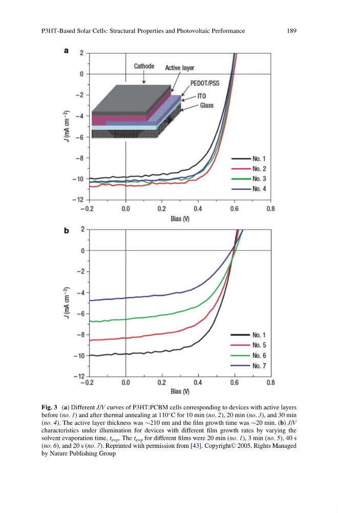
Fig. 3 (a) Different J/V curves of P3HT:PCBM cells corresponding to devices with active layers
before (no. 1) and after thermal annealing at 110
C for 10 min (no. 2), 20 min (no. 3), and 30 min
(no. 4). The active layer thickness was $210 nm and the film growth time was $20 min. (b) J/V
characteristics under illumination for devices with different film growth rates by varying the
solvent evaporation time, t evp . The t evp for different films were 20 min (no. 1), 3 min (no. 5), 40 s
(no. 6), and 20 s (no. 7). Reprinted with permission from [43]. Copyright© 2005, Rights Managed
by Nature Publishing Group
P3HT-Based Solar Cells: Structural Properties and Photovoltaic Performance
189
before (no. 1) and after thermal annealing at 110
C for 10 min (no. 2), 20 min (no. 3), and 30 min
(no. 4). The active layer thickness was $210 nm and the film growth time was $20 min. (b) J/V
characteristics under illumination for devices with different film growth rates by varying the
solvent evaporation time, t evp . The t evp for different films were 20 min (no. 1), 3 min (no. 5), 40 s
(no. 6), and 20 s (no. 7). Reprinted with permission from [43]. Copyright© 2005, Rights Managed
by Nature Publishing Group
P3HT-Based Solar Cells: Structural Properties and Photovoltaic Performance
189