

3.2 Folded Chain Versus Extended Chain Crystallization
Macromolecular parameters like M w and the regioregularity of P3HT are known to
significantly affect charge transport properties in thin films [67, 68]. Various groups
have investigated the correlations between the morphology observed by atomic
force microscopy (AFM) in spin-coated films and the corresponding hole mobility
in organic field-effect transistors (OFETs). It is reported that low-M w P3HT forms
well-defined nanofibrillar domains but exhibits poor hole mobility, whereas P3HT
with M w ! 20 kDa yields thin films with poorly defined morphologies and significantly higher charge carrier mobilities. As a rationale, Kline proposed the existence of tie-chains linking successive crystalline domains via some poorly ordered
amorphous zones [67]. With increasing M w , one can expect an increasing proportion of such tie chains. Although AFM gave clear evidence for the formation of
P3HT nanofibrils in thin films, the distinction between amorphous and crystalline
domains was difficult [67]. Distinction was, however, possible by using TEM on
epitaxied thin films [43, 44]. Therefore, by growing oriented films of P3HT by
epitaxy, it is possible to investigate the influence of M w on the semicrystalline
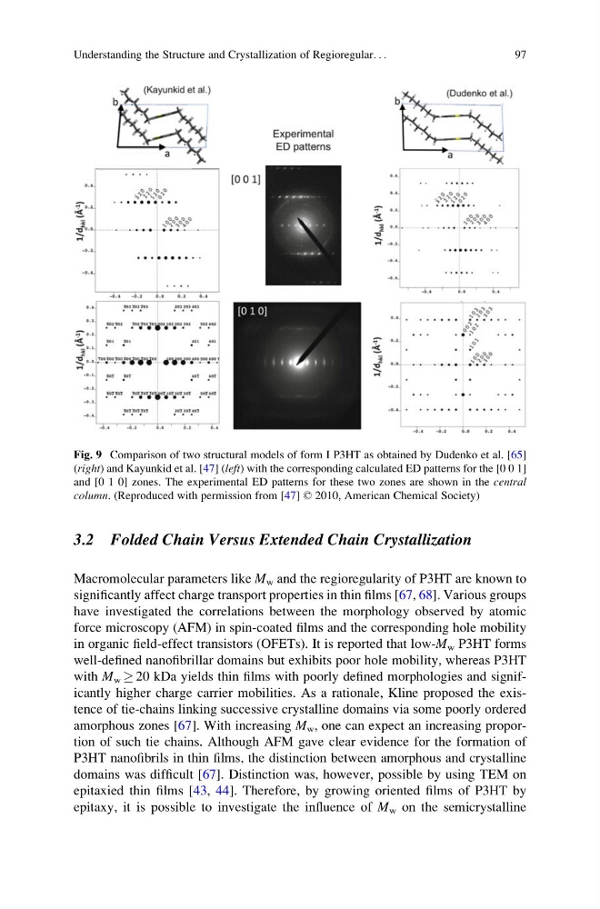
Fig. 9 Comparison of two structural models of form I P3HT as obtained by Dudenko et al. [65]
(right) and Kayunkid et al. [47] (left) with the corresponding calculated ED patterns for the [0 0 1]
and [0 1 0] zones. The experimental ED patterns for these two zones are shown in the central
column. (Reproduced with permission from [47] © 2010, American Chemical Society)
Understanding the Structure and Crystallization of Regioregular. . .
97
Macromolecular parameters like M w and the regioregularity of P3HT are known to
significantly affect charge transport properties in thin films [67, 68]. Various groups
have investigated the correlations between the morphology observed by atomic
force microscopy (AFM) in spin-coated films and the corresponding hole mobility
in organic field-effect transistors (OFETs). It is reported that low-M w P3HT forms
well-defined nanofibrillar domains but exhibits poor hole mobility, whereas P3HT
with M w ! 20 kDa yields thin films with poorly defined morphologies and significantly higher charge carrier mobilities. As a rationale, Kline proposed the existence of tie-chains linking successive crystalline domains via some poorly ordered
amorphous zones [67]. With increasing M w , one can expect an increasing proportion of such tie chains. Although AFM gave clear evidence for the formation of
P3HT nanofibrils in thin films, the distinction between amorphous and crystalline
domains was difficult [67]. Distinction was, however, possible by using TEM on
epitaxied thin films [43, 44]. Therefore, by growing oriented films of P3HT by
epitaxy, it is possible to investigate the influence of M w on the semicrystalline
Fig. 9 Comparison of two structural models of form I P3HT as obtained by Dudenko et al. [65]
(right) and Kayunkid et al. [47] (left) with the corresponding calculated ED patterns for the [0 0 1]
and [0 1 0] zones. The experimental ED patterns for these two zones are shown in the central
column. (Reproduced with permission from [47] © 2010, American Chemical Society)
Understanding the Structure and Crystallization of Regioregular. . .
97