

82
4 Ultrathin Layers
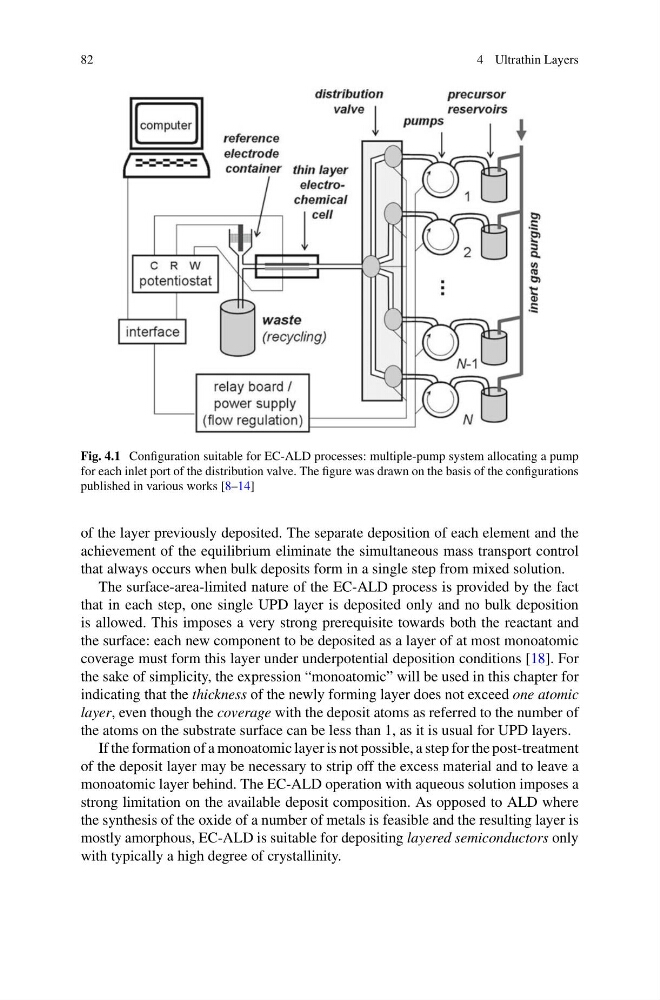
Fig. 4.1 Configuration suitable for EC-ALD processes: multiple-pump system allocating a pump
for each inlet port of the distribution valve. The figure was drawn on the basis of the configurations
published in various works [8–14]
of the layer previously deposited. The separate deposition of each element and the
achievement of the equilibrium eliminate the simultaneous mass transport control
that always occurs when bulk deposits form in a single step from mixed solution.
The surface-area-limited nature of the EC-ALD process is provided by the fact
that in each step, one single UPD layer is deposited only and no bulk deposition
is allowed. This imposes a very strong prerequisite towards both the reactant and
the surface: each new component to be deposited as a layer of at most monoatomic
coverage must form this layer under underpotential deposition conditions [18]. For
the sake of simplicity, the expression “monoatomic” will be used in this chapter for
indicating that the thickness of the newly forming layer does not exceed one atomic
layer, even though the coverage with the deposit atoms as referred to the number of
the atoms on the substrate surface can be less than 1, as it is usual for UPD layers.
If the formation of a monoatomic layer is not possible, a step for the post-treatment
of the deposit layer may be necessary to strip off the excess material and to leave a
monoatomic layer behind. The EC-ALD operation with aqueous solution imposes a
strong limitation on the available deposit composition. As opposed to ALD where
the synthesis of the oxide of a number of metals is feasible and the resulting layer is
mostly amorphous, EC-ALD is suitable for depositing layered semiconductors only
with typically a high degree of crystallinity.
4 Ultrathin Layers
Fig. 4.1 Configuration suitable for EC-ALD processes: multiple-pump system allocating a pump
for each inlet port of the distribution valve. The figure was drawn on the basis of the configurations
published in various works [8–14]
of the layer previously deposited. The separate deposition of each element and the
achievement of the equilibrium eliminate the simultaneous mass transport control
that always occurs when bulk deposits form in a single step from mixed solution.
The surface-area-limited nature of the EC-ALD process is provided by the fact
that in each step, one single UPD layer is deposited only and no bulk deposition
is allowed. This imposes a very strong prerequisite towards both the reactant and
the surface: each new component to be deposited as a layer of at most monoatomic
coverage must form this layer under underpotential deposition conditions [18]. For
the sake of simplicity, the expression “monoatomic” will be used in this chapter for
indicating that the thickness of the newly forming layer does not exceed one atomic
layer, even though the coverage with the deposit atoms as referred to the number of
the atoms on the substrate surface can be less than 1, as it is usual for UPD layers.
If the formation of a monoatomic layer is not possible, a step for the post-treatment
of the deposit layer may be necessary to strip off the excess material and to leave a
monoatomic layer behind. The EC-ALD operation with aqueous solution imposes a
strong limitation on the available deposit composition. As opposed to ALD where
the synthesis of the oxide of a number of metals is feasible and the resulting layer is
mostly amorphous, EC-ALD is suitable for depositing layered semiconductors only
with typically a high degree of crystallinity.