

72
3 Experimental Methods in Characterization of Nanosystems
Scanning tunnelling microscopy (STM) applies atomically sharp tips. The
measured parameter is the tunnelling current between the conductive surface of
the test specimen and the tip. The tunnelling current depends exponentially on the
distance between the tip and the surface and is linearly proportional to the energydependent electronic density of states of the sample surface. Since the density of
state strongly varies at much smaller scale than the size of a single atom, the atomic
structure of a conducting surface can be mapped with subatomic resolution. Specific
features on single-crystal surfaces detectable with STM include surface defects,
steps and terrace edges, and binding mode and configuration of adsorbed molecules
including their conformation. For surfaces that are not atomically smooth, the estimation of surface roughness is a prominent application mode of STM. The constantcurrent operation is typical for STM. In electrochemical environment (i.e., under
solution and with electrode potential control), combined apparatus with potentiostatic control of the specimen surface is required in combination of the potential
difference regulation between the tip and the surface scanned by an integrated highsensitivity electronic device. In vacuum or in air, the side of the tip is of no importance,
while in electrochemical STM mode, it has to be covered nearly to the very end of
the tip so that to reduce parasite current as much as possible. A variation of STM is
scanning tunnelling spectroscopy where the potential difference between the tip and
the specimen is also modulated, and the detection of local tunnelling conductance
yields a local excitation spectrum.
Atomic force microscopy (AFM) applies tips of 5–25 nm end radius. Since the
measured parameter is the force acting between the tip and the specimen surface,
the tip does not have to be electrically conductive. The most common material for
commercially available tips is silicon nitride for which the half-angle of the tips
is around 20°. Sharper ceramic tips with a half-angle of a few degree and curvatures down to the 1-nm-level are available with special manufacturing techniques,
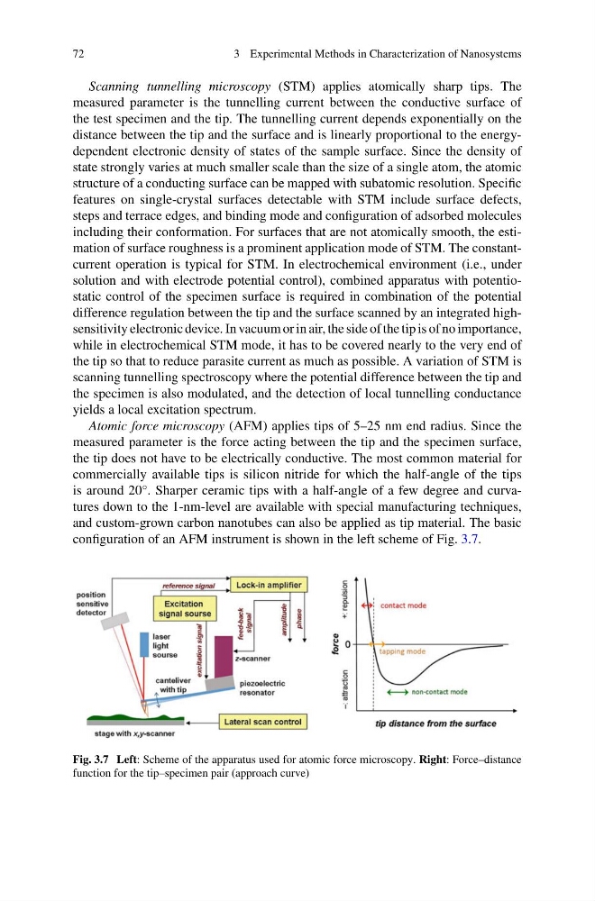
and custom-grown carbon nanotubes can also be applied as tip material. The basic
configuration of an AFM instrument is shown in the left scheme of Fig. 3.7.
Fig. 3.7 Left: Scheme of the apparatus used for atomic force microscopy. Right: Force–distance
function for the tip–specimen pair (approach curve)
3 Experimental Methods in Characterization of Nanosystems
Scanning tunnelling microscopy (STM) applies atomically sharp tips. The
measured parameter is the tunnelling current between the conductive surface of
the test specimen and the tip. The tunnelling current depends exponentially on the
distance between the tip and the surface and is linearly proportional to the energydependent electronic density of states of the sample surface. Since the density of
state strongly varies at much smaller scale than the size of a single atom, the atomic
structure of a conducting surface can be mapped with subatomic resolution. Specific
features on single-crystal surfaces detectable with STM include surface defects,
steps and terrace edges, and binding mode and configuration of adsorbed molecules
including their conformation. For surfaces that are not atomically smooth, the estimation of surface roughness is a prominent application mode of STM. The constantcurrent operation is typical for STM. In electrochemical environment (i.e., under
solution and with electrode potential control), combined apparatus with potentiostatic control of the specimen surface is required in combination of the potential
difference regulation between the tip and the surface scanned by an integrated highsensitivity electronic device. In vacuum or in air, the side of the tip is of no importance,
while in electrochemical STM mode, it has to be covered nearly to the very end of
the tip so that to reduce parasite current as much as possible. A variation of STM is
scanning tunnelling spectroscopy where the potential difference between the tip and
the specimen is also modulated, and the detection of local tunnelling conductance
yields a local excitation spectrum.
Atomic force microscopy (AFM) applies tips of 5–25 nm end radius. Since the
measured parameter is the force acting between the tip and the specimen surface,
the tip does not have to be electrically conductive. The most common material for
commercially available tips is silicon nitride for which the half-angle of the tips
is around 20°. Sharper ceramic tips with a half-angle of a few degree and curvatures down to the 1-nm-level are available with special manufacturing techniques,
and custom-grown carbon nanotubes can also be applied as tip material. The basic
configuration of an AFM instrument is shown in the left scheme of Fig. 3.7.
Fig. 3.7 Left: Scheme of the apparatus used for atomic force microscopy. Right: Force–distance
function for the tip–specimen pair (approach curve)