

336
10 Electrochemical Manufacturing Methods Based on Surface …
a
b
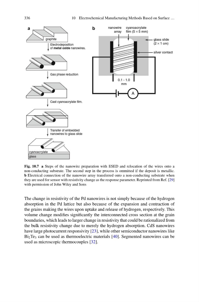
Fig. 10.7 a Steps of the nanowire preparation with ESED and relocation of the wires onto a
non-conducting substrate. The second step in the process is ommitted if the deposit is metallic.
b Electrical connection of the nanowire array transferred onto a non-conducting substrate when
they are used for sensor with resistivity change as the response parameter. Reprinted from Ref. [29]
with permission of John Wiley and Sons
The change in resistivity of the Pd nanowires is not simply because of the hydrogen
absorption in the Pd lattice but also because of the expansion and contraction of
the grains making the wires upon uptake and release of hydrogen, respectively. This
volume change modifies significantly the interconnected cross section at the grain
boundaries, which leads to larger change in resistivity that could be rationalized from
the bulk resistivity change due to merely the hydrogen absorption. CdS nanowires
have large photocurrent responsivity [23], while other semiconductor nanowires like
Bi 2 Te 3 can be used as thermoelectric materials [40]. Segmented nanowires can be
used as microscopic thermocouples [32].
10 Electrochemical Manufacturing Methods Based on Surface …
a
b
Fig. 10.7 a Steps of the nanowire preparation with ESED and relocation of the wires onto a
non-conducting substrate. The second step in the process is ommitted if the deposit is metallic.
b Electrical connection of the nanowire array transferred onto a non-conducting substrate when
they are used for sensor with resistivity change as the response parameter. Reprinted from Ref. [29]
with permission of John Wiley and Sons
The change in resistivity of the Pd nanowires is not simply because of the hydrogen
absorption in the Pd lattice but also because of the expansion and contraction of
the grains making the wires upon uptake and release of hydrogen, respectively. This
volume change modifies significantly the interconnected cross section at the grain
boundaries, which leads to larger change in resistivity that could be rationalized from
the bulk resistivity change due to merely the hydrogen absorption. CdS nanowires
have large photocurrent responsivity [23], while other semiconductor nanowires like
Bi 2 Te 3 can be used as thermoelectric materials [40]. Segmented nanowires can be
used as microscopic thermocouples [32].