

334
10 Electrochemical Manufacturing Methods Based on Surface …
after the electrodeposition. The MnO 2 wires were of granular structure, similar to
metal nanowires obtained with ESED.
In a few cases, metal oxide nanowires can be produced from solutions containing
simple metal cations (i.e., not oxoanions). As it is usually done with CuSO 4 solutions
to obtain Cu 2 O nanocrystals, the ESED synthesis of Cu 2 O nanowires is possible
when the solution is quite dilute and unbuffered [26]. For the production of Ag x O,
deposition can be carried with anodic oxidation of Ag
+ from a nearly neutral acetate
solution [38]. The composition of the deposit exhibited some uncertainty concerning
the oxidation state of silver, and the result of various characterization methods was
in acceptable agreement with Ag 2 O, too.
As an example for the ESED with a semiconductor obtained by direct deposition,
the formation of Bi 2 Te 3 can be mentioned [39, 40]. The deposition conditions of
Bi 2 Te 3 are similar to those mentioned in Chap. 4 (i.e., solutions with at most a
few mM precursor concentrations). An important difference as compared to other
ESED processes is that the single-step deposition of Bi 2 Te 3 is not possible. For this
reason, the pulse sequence shown in Fig. 10.1 was slightly modified. After the anodic
pre-treatment and the cathodic nucleation pulses, the deposition could be performed
with running subsequent cyclic voltammograms in the potential range comprising the
UPD region of both components. The anodic limit was positive enough to strip off the
excess Bi and hence to achieve the desired composition. A similar process was proved
to be feasible fore CdSe nanowire deposition by ESED [41]. The major difference was
that the desired composition could be achieved by running the voltammograms during
the deposition process in an unusually wide 1.4 V potential interval to achieve the
stripping of the excess of both components. For indirect preparation of semiconductor
nanowires along the surface, the reaction of Cd deposits with H 2 S opens the way for
CdS nanowire formation [23].
Concerning the kinetics of the nanowire growth along the step edge, it was found
for essentially all deposits that they exhibit a hemicylindrical shape. Assuming that
(i) the accumulated length of the step edges along which the growth takes place
does not vary in time, (ii) the coalescence of the particles forming the nanowires
takes place early enough during the nanowire growth (or, at least, the overlap of the
diffusion field takes place shortly after their nucleation), (iii) the growth process is
controlled by the diffusion of the precursor ions, the current is expected to reach a
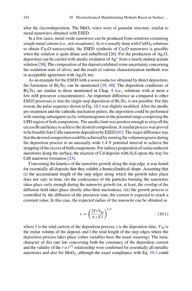
constant value. In this case, the expected radius of the nanowire can be obtained as
r =
2I tV M
π z F l
1/2
(10.1)
where I is the total current of the deposition process, t is the deposition time, V M is
the molar volume of the deposit, and l the total length of the step edges where the
deposition process takes place (other variables have the usual meaning). The basic
character of this rate law concerning both the constancy of the deposition current
and the validity of the r α t
1/2 relationship were confirmed for essentially all metallic
nanowires and also for MoO 2 , although the exact compliance with Eq. 10.1 could
10 Electrochemical Manufacturing Methods Based on Surface …
after the electrodeposition. The MnO 2 wires were of granular structure, similar to
metal nanowires obtained with ESED.
In a few cases, metal oxide nanowires can be produced from solutions containing
simple metal cations (i.e., not oxoanions). As it is usually done with CuSO 4 solutions
to obtain Cu 2 O nanocrystals, the ESED synthesis of Cu 2 O nanowires is possible
when the solution is quite dilute and unbuffered [26]. For the production of Ag x O,
deposition can be carried with anodic oxidation of Ag
+ from a nearly neutral acetate
solution [38]. The composition of the deposit exhibited some uncertainty concerning
the oxidation state of silver, and the result of various characterization methods was
in acceptable agreement with Ag 2 O, too.
As an example for the ESED with a semiconductor obtained by direct deposition,
the formation of Bi 2 Te 3 can be mentioned [39, 40]. The deposition conditions of
Bi 2 Te 3 are similar to those mentioned in Chap. 4 (i.e., solutions with at most a
few mM precursor concentrations). An important difference as compared to other
ESED processes is that the single-step deposition of Bi 2 Te 3 is not possible. For this
reason, the pulse sequence shown in Fig. 10.1 was slightly modified. After the anodic
pre-treatment and the cathodic nucleation pulses, the deposition could be performed
with running subsequent cyclic voltammograms in the potential range comprising the
UPD region of both components. The anodic limit was positive enough to strip off the
excess Bi and hence to achieve the desired composition. A similar process was proved
to be feasible fore CdSe nanowire deposition by ESED [41]. The major difference was
that the desired composition could be achieved by running the voltammograms during
the deposition process in an unusually wide 1.4 V potential interval to achieve the
stripping of the excess of both components. For indirect preparation of semiconductor
nanowires along the surface, the reaction of Cd deposits with H 2 S opens the way for
CdS nanowire formation [23].
Concerning the kinetics of the nanowire growth along the step edge, it was found
for essentially all deposits that they exhibit a hemicylindrical shape. Assuming that
(i) the accumulated length of the step edges along which the growth takes place
does not vary in time, (ii) the coalescence of the particles forming the nanowires
takes place early enough during the nanowire growth (or, at least, the overlap of the
diffusion field takes place shortly after their nucleation), (iii) the growth process is
controlled by the diffusion of the precursor ions, the current is expected to reach a
constant value. In this case, the expected radius of the nanowire can be obtained as
r =
2I tV M
π z F l
1/2
(10.1)
where I is the total current of the deposition process, t is the deposition time, V M is
the molar volume of the deposit, and l the total length of the step edges where the
deposition process takes place (other variables have the usual meaning). The basic
character of this rate law concerning both the constancy of the deposition current
and the validity of the r α t
1/2 relationship were confirmed for essentially all metallic
nanowires and also for MoO 2 , although the exact compliance with Eq. 10.1 could