

188
6 Nanocrystalline Deposits
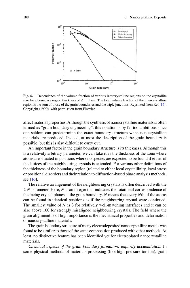
Fig. 6.1 Dependence of the volume fraction of various intercrystalline regions on the crystallite
size for a boundary region thickness of Δ = 1 nm. The total volume fraction of the intercrystalline
region is the sum of those of the grain boundaries and the triple junctions. Reprinted from Ref [15].
Copyright (1990), with permission from Elsevier
affect material properties. Although the synthesis of nanocrystalline materials is often
termed as “grain boundary engineering”, this notation is by far too ambitious since
one seldom can predetermine the exact boundary structure when nanocrystalline
materials are produced. Instead, at most the description of the grain boundary is
possible, but this is also difficult to carry out.
An important factor in the grain boundary structure is its thickness. Although this
is a relatively arbitrary parameter, we can take it as the thickness of the zone where
atoms are situated in positions where no species are expected to be found if either of
the lattices of the neighbouring crystals is extended. For various other definitions of
the thickness of the boundary region (related to either local crystallinity, local stress
or positional disorder) and their relation to diffraction-based phase analysis methods,
see [16].
The relative arrangement of the neighbouring crystals is often described with the
N parameter. Here, N is an integer that indicates the rotational correspondence of
the facing crystal planes at the grain boundary. N means that every Nth of the atoms
can be found in identical positions as if the neighbouring crystal were continued.
The smallest value of N is 3 for relatively well-matching interfaces and it can be
also above 100 for strongly misaligned neighbouring crystals. The field where the
grain alignment is of high importance is the mechanical properties and deformation
of nanocrystalline materials.
The grain boundary structure of many electrodeposited nanocrystalline metals was
found to be similar to those of the same composition produced with other methods. At
least, no distinctive feature has been identified yet for electroplated nanocrystalline
materials.
Chemical aspects of the grain boundary formation: impurity accumulation. In
some physical methods of materials processing (like high-pressure torsion), grain
6 Nanocrystalline Deposits
Fig. 6.1 Dependence of the volume fraction of various intercrystalline regions on the crystallite
size for a boundary region thickness of Δ = 1 nm. The total volume fraction of the intercrystalline
region is the sum of those of the grain boundaries and the triple junctions. Reprinted from Ref [15].
Copyright (1990), with permission from Elsevier
affect material properties. Although the synthesis of nanocrystalline materials is often
termed as “grain boundary engineering”, this notation is by far too ambitious since
one seldom can predetermine the exact boundary structure when nanocrystalline
materials are produced. Instead, at most the description of the grain boundary is
possible, but this is also difficult to carry out.
An important factor in the grain boundary structure is its thickness. Although this
is a relatively arbitrary parameter, we can take it as the thickness of the zone where
atoms are situated in positions where no species are expected to be found if either of
the lattices of the neighbouring crystals is extended. For various other definitions of
the thickness of the boundary region (related to either local crystallinity, local stress
or positional disorder) and their relation to diffraction-based phase analysis methods,
see [16].
The relative arrangement of the neighbouring crystals is often described with the
N parameter. Here, N is an integer that indicates the rotational correspondence of
the facing crystal planes at the grain boundary. N means that every Nth of the atoms
can be found in identical positions as if the neighbouring crystal were continued.
The smallest value of N is 3 for relatively well-matching interfaces and it can be
also above 100 for strongly misaligned neighbouring crystals. The field where the
grain alignment is of high importance is the mechanical properties and deformation
of nanocrystalline materials.
The grain boundary structure of many electrodeposited nanocrystalline metals was
found to be similar to those of the same composition produced with other methods. At
least, no distinctive feature has been identified yet for electroplated nanocrystalline
materials.
Chemical aspects of the grain boundary formation: impurity accumulation. In
some physical methods of materials processing (like high-pressure torsion), grain