

186
6 Nanocrystalline Deposits
drive the deposition process away from the near-equilibrium growth also lead to
grain refinement. Most importantly, the application of additives has to be mentioned.
Additives block the near-equilibrium growth sites (kink points, edges and screw
dislocations), hence allowing adatom accumulation on the terrace plane surfaces.
Since the nucleation of new crystals takes place via random processes, fine-grained
deposits exhibit much weaker texture than coarse-grained ones. Another collateral
advantage of the reduction of the crystallite size is that the deposits become smoother
due to the lack of the preferential growth points and the suppression of the dendrite
formation.
Pulse plating is often applied for obtaining nanocrystalline deposits. The advantage of pulse plating is that the current density applied during the on-time can be
much larger than the mass transport-limited current density during d.c. plating. The
shorter the on-time period, the larger current density can be applied; however, a
sufficiently long off-time is required for the replenishment of the reactant by diffusion. The convenient calculation mode for treating the length of the on-time, t ON , the
duty cycle, θ = t ON /(t ON + t OFF ), and the pulse-limiting current density for currentcontrolled deposition, j PG is based on the double diffusion layer approximation [13,
14]. Here, the maximum pulse length is limited by the achievement of the zero reactant concentration at the cathode surface by the end of the pulse. The dimensionless
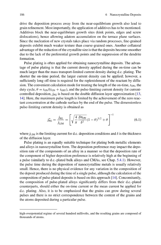
pulse-limiting current density is obtained as
j
∗
PG =
j PG
j LIM
=
4
π
Dt ON
δ 2 (1 − θ )
3/2
+ θ
−1
(6.1)
where j LIM is the limiting current for d.c. deposition conditions and δ is the thickness
of the diffusion layer.
Pulse plating is an equally suitable technique for plating both metallic elements
and alloys in nanocrystalline form. The deposition preference may impact the deposition rate of the components of an alloy in a manner so that the deposition rate of
the component of higher deposition preference is relatively high at the beginning of
a pulse (similarly to d.c.-plated bulk alloys and CMAs, see Chap. 5.4.1). However,
the pulse time during the deposition of nanocrystalline metals is usually relatively
small. Hence, there is no physical evidence for any variation in the composition of
the deposit produced during the time of a single pulse, although the calculation of the
composition of pulse-plated deposits is based on this approach [14]. Concomitantly,
the composition of pulse-plated alloys significantly differs from their d.c.-plated
counterparts, should either the on-time current or the mean current be applied for
d.c. plating. Also, it is to be emphasized that the grains can grow during several
pulses and there is no strict correspondence between the content of the grains and
the atoms deposited during a particular pulse.
high-overpotential regime of several hundred millivolts, and the resulting grains are composed of
thousands of atoms.
6 Nanocrystalline Deposits
drive the deposition process away from the near-equilibrium growth also lead to
grain refinement. Most importantly, the application of additives has to be mentioned.
Additives block the near-equilibrium growth sites (kink points, edges and screw
dislocations), hence allowing adatom accumulation on the terrace plane surfaces.
Since the nucleation of new crystals takes place via random processes, fine-grained
deposits exhibit much weaker texture than coarse-grained ones. Another collateral
advantage of the reduction of the crystallite size is that the deposits become smoother
due to the lack of the preferential growth points and the suppression of the dendrite
formation.
Pulse plating is often applied for obtaining nanocrystalline deposits. The advantage of pulse plating is that the current density applied during the on-time can be
much larger than the mass transport-limited current density during d.c. plating. The
shorter the on-time period, the larger current density can be applied; however, a
sufficiently long off-time is required for the replenishment of the reactant by diffusion. The convenient calculation mode for treating the length of the on-time, t ON , the
duty cycle, θ = t ON /(t ON + t OFF ), and the pulse-limiting current density for currentcontrolled deposition, j PG is based on the double diffusion layer approximation [13,
14]. Here, the maximum pulse length is limited by the achievement of the zero reactant concentration at the cathode surface by the end of the pulse. The dimensionless
pulse-limiting current density is obtained as
j
∗
PG =
j PG
j LIM
=
4
π
Dt ON
δ 2 (1 − θ )
3/2
+ θ
−1
(6.1)
where j LIM is the limiting current for d.c. deposition conditions and δ is the thickness
of the diffusion layer.
Pulse plating is an equally suitable technique for plating both metallic elements
and alloys in nanocrystalline form. The deposition preference may impact the deposition rate of the components of an alloy in a manner so that the deposition rate of
the component of higher deposition preference is relatively high at the beginning of
a pulse (similarly to d.c.-plated bulk alloys and CMAs, see Chap. 5.4.1). However,
the pulse time during the deposition of nanocrystalline metals is usually relatively
small. Hence, there is no physical evidence for any variation in the composition of
the deposit produced during the time of a single pulse, although the calculation of the
composition of pulse-plated deposits is based on this approach [14]. Concomitantly,
the composition of pulse-plated alloys significantly differs from their d.c.-plated
counterparts, should either the on-time current or the mean current be applied for
d.c. plating. Also, it is to be emphasized that the grains can grow during several
pulses and there is no strict correspondence between the content of the grains and
the atoms deposited during a particular pulse.
high-overpotential regime of several hundred millivolts, and the resulting grains are composed of
thousands of atoms.