

5.4 Properties of Electrodeposited CMAs
157
thicknesses slightly larger than 1 nm. Co/Ag two-pulse-plated deposits show much
smaller ordered zones, and Co/Pb deposits are fully granular at any nominal layer
thickness.
When layers with dissimilar composition are plated onto each other with repeat
periods less than the crystallite size, the composition modulation is usually independent of the crystallite size and shape of the deposit (i.e., whether the deposit is
composed of large columnar crystals or equiaxed nanograins). This was well exemplified for Ni/Cu multilayers [95]. For the Ni/Cu system, the choice of the Cu deposition
current density (or electrode potential) has some freedom since the partial polarization curve corresponding to the nickel dissolution has the onset at more positive
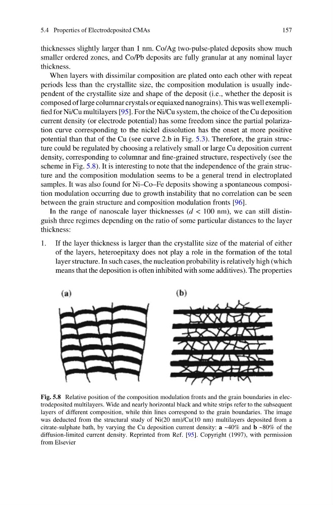
potential than that of the Cu (see curve 2.b in Fig. 5.3). Therefore, the grain structure could be regulated by choosing a relatively small or large Cu deposition current
density, corresponding to columnar and fine-grained structure, respectively (see the
scheme in Fig. 5.8). It is interesting to note that the independence of the grain structure and the composition modulation seems to be a general trend in electroplated
samples. It was also found for Ni–Co–Fe deposits showing a spontaneous composition modulation occurring due to growth instability that no correlation can be seen
between the grain structure and composition modulation fronts [96].
In the range of nanoscale layer thicknesses (d < 100 nm), we can still distinguish three regimes depending on the ratio of some particular distances to the layer
thickness:
1. If the layer thickness is larger than the crystallite size of the material of either
of the layers, heteroepitaxy does not play a role in the formation of the total
layer structure. In such cases, the nucleation probability is relatively high (which
means that the deposition is often inhibited with some additives). The properties
Fig. 5.8 Relative position of the composition modulation fronts and the grain boundaries in electrodeposited multilayers. Wide and nearly horizontal black and white strips refer to the subsequent
layers of different composition, while thin lines correspond to the grain boundaries. The image
was deducted from the structural study of Ni(20 nm)/Cu(10 nm) multilayers deposited from a
citrate-sulphate bath, by varying the Cu deposition current density: a ~40% and b ~80% of the
diffusion-limited current density. Reprinted from Ref. [95]. Copyright (1997), with permission
from Elsevier
157
thicknesses slightly larger than 1 nm. Co/Ag two-pulse-plated deposits show much
smaller ordered zones, and Co/Pb deposits are fully granular at any nominal layer
thickness.
When layers with dissimilar composition are plated onto each other with repeat
periods less than the crystallite size, the composition modulation is usually independent of the crystallite size and shape of the deposit (i.e., whether the deposit is
composed of large columnar crystals or equiaxed nanograins). This was well exemplified for Ni/Cu multilayers [95]. For the Ni/Cu system, the choice of the Cu deposition
current density (or electrode potential) has some freedom since the partial polarization curve corresponding to the nickel dissolution has the onset at more positive
potential than that of the Cu (see curve 2.b in Fig. 5.3). Therefore, the grain structure could be regulated by choosing a relatively small or large Cu deposition current
density, corresponding to columnar and fine-grained structure, respectively (see the
scheme in Fig. 5.8). It is interesting to note that the independence of the grain structure and the composition modulation seems to be a general trend in electroplated
samples. It was also found for Ni–Co–Fe deposits showing a spontaneous composition modulation occurring due to growth instability that no correlation can be seen
between the grain structure and composition modulation fronts [96].
In the range of nanoscale layer thicknesses (d < 100 nm), we can still distinguish three regimes depending on the ratio of some particular distances to the layer
thickness:
1. If the layer thickness is larger than the crystallite size of the material of either
of the layers, heteroepitaxy does not play a role in the formation of the total
layer structure. In such cases, the nucleation probability is relatively high (which
means that the deposition is often inhibited with some additives). The properties
Fig. 5.8 Relative position of the composition modulation fronts and the grain boundaries in electrodeposited multilayers. Wide and nearly horizontal black and white strips refer to the subsequent
layers of different composition, while thin lines correspond to the grain boundaries. The image
was deducted from the structural study of Ni(20 nm)/Cu(10 nm) multilayers deposited from a
citrate-sulphate bath, by varying the Cu deposition current density: a ~40% and b ~80% of the
diffusion-limited current density. Reprinted from Ref. [95]. Copyright (1997), with permission
from Elsevier