

136
5 Compositionally Modulated and Multilayered Deposits
a
b
c
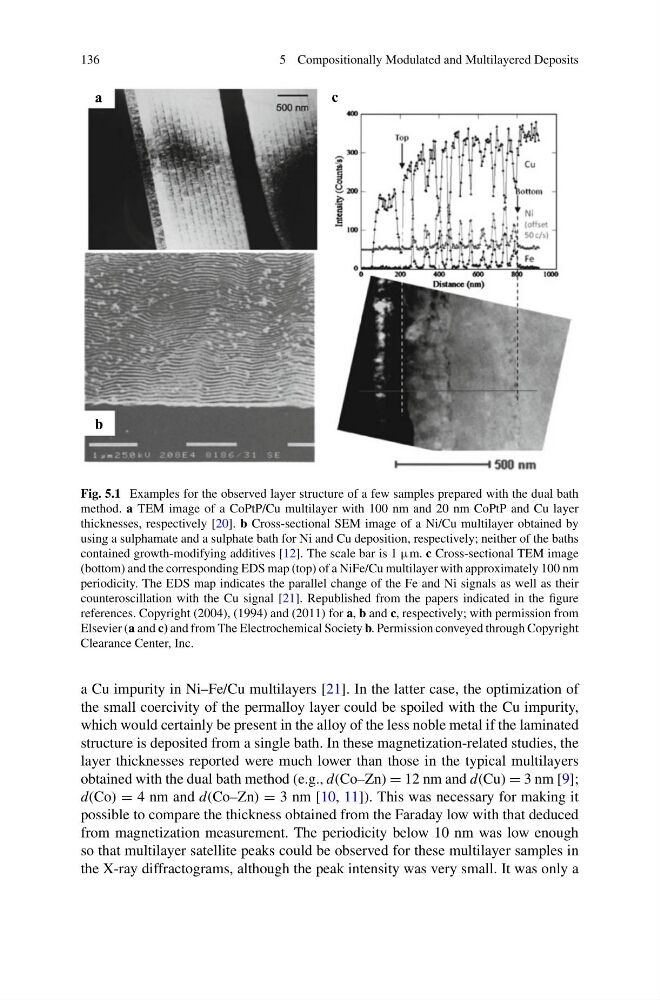
Fig. 5.1 Examples for the observed layer structure of a few samples prepared with the dual bath
method. a TEM image of a CoPtP/Cu multilayer with 100 nm and 20 nm CoPtP and Cu layer
thicknesses, respectively [20]. b Cross-sectional SEM image of a Ni/Cu multilayer obtained by
using a sulphamate and a sulphate bath for Ni and Cu deposition, respectively; neither of the baths
contained growth-modifying additives [12]. The scale bar is 1 μm. c Cross-sectional TEM image
(bottom) and the corresponding EDS map (top) of a NiFe/Cu multilayer with approximately 100 nm
periodicity. The EDS map indicates the parallel change of the Fe and Ni signals as well as their
counteroscillation with the Cu signal [21]. Republished from the papers indicated in the figure
references. Copyright (2004), (1994) and (2011) for a, b and c, respectively; with permission from
Elsevier (a and c) and from The Electrochemical Society b. Permission conveyed through Copyright
Clearance Center, Inc.
a Cu impurity in Ni–Fe/Cu multilayers [21]. In the latter case, the optimization of
the small coercivity of the permalloy layer could be spoiled with the Cu impurity,
which would certainly be present in the alloy of the less noble metal if the laminated
structure is deposited from a single bath. In these magnetization-related studies, the
layer thicknesses reported were much lower than those in the typical multilayers
obtained with the dual bath method (e.g., d(Co–Zn) = 12 nm and d(Cu) = 3 nm [9];
d(Co) = 4 nm and d(Co–Zn) = 3 nm [10, 11]). This was necessary for making it
possible to compare the thickness obtained from the Faraday low with that deduced
from magnetization measurement. The periodicity below 10 nm was low enough
so that multilayer satellite peaks could be observed for these multilayer samples in
the X-ray diffractograms, although the peak intensity was very small. It was only a
5 Compositionally Modulated and Multilayered Deposits
a
b
c
Fig. 5.1 Examples for the observed layer structure of a few samples prepared with the dual bath
method. a TEM image of a CoPtP/Cu multilayer with 100 nm and 20 nm CoPtP and Cu layer
thicknesses, respectively [20]. b Cross-sectional SEM image of a Ni/Cu multilayer obtained by
using a sulphamate and a sulphate bath for Ni and Cu deposition, respectively; neither of the baths
contained growth-modifying additives [12]. The scale bar is 1 μm. c Cross-sectional TEM image
(bottom) and the corresponding EDS map (top) of a NiFe/Cu multilayer with approximately 100 nm
periodicity. The EDS map indicates the parallel change of the Fe and Ni signals as well as their
counteroscillation with the Cu signal [21]. Republished from the papers indicated in the figure
references. Copyright (2004), (1994) and (2011) for a, b and c, respectively; with permission from
Elsevier (a and c) and from The Electrochemical Society b. Permission conveyed through Copyright
Clearance Center, Inc.
a Cu impurity in Ni–Fe/Cu multilayers [21]. In the latter case, the optimization of
the small coercivity of the permalloy layer could be spoiled with the Cu impurity,
which would certainly be present in the alloy of the less noble metal if the laminated
structure is deposited from a single bath. In these magnetization-related studies, the
layer thicknesses reported were much lower than those in the typical multilayers
obtained with the dual bath method (e.g., d(Co–Zn) = 12 nm and d(Cu) = 3 nm [9];
d(Co) = 4 nm and d(Co–Zn) = 3 nm [10, 11]). This was necessary for making it
possible to compare the thickness obtained from the Faraday low with that deduced
from magnetization measurement. The periodicity below 10 nm was low enough
so that multilayer satellite peaks could be observed for these multilayer samples in
the X-ray diffractograms, although the peak intensity was very small. It was only a