

96
4 Ultrathin Layers
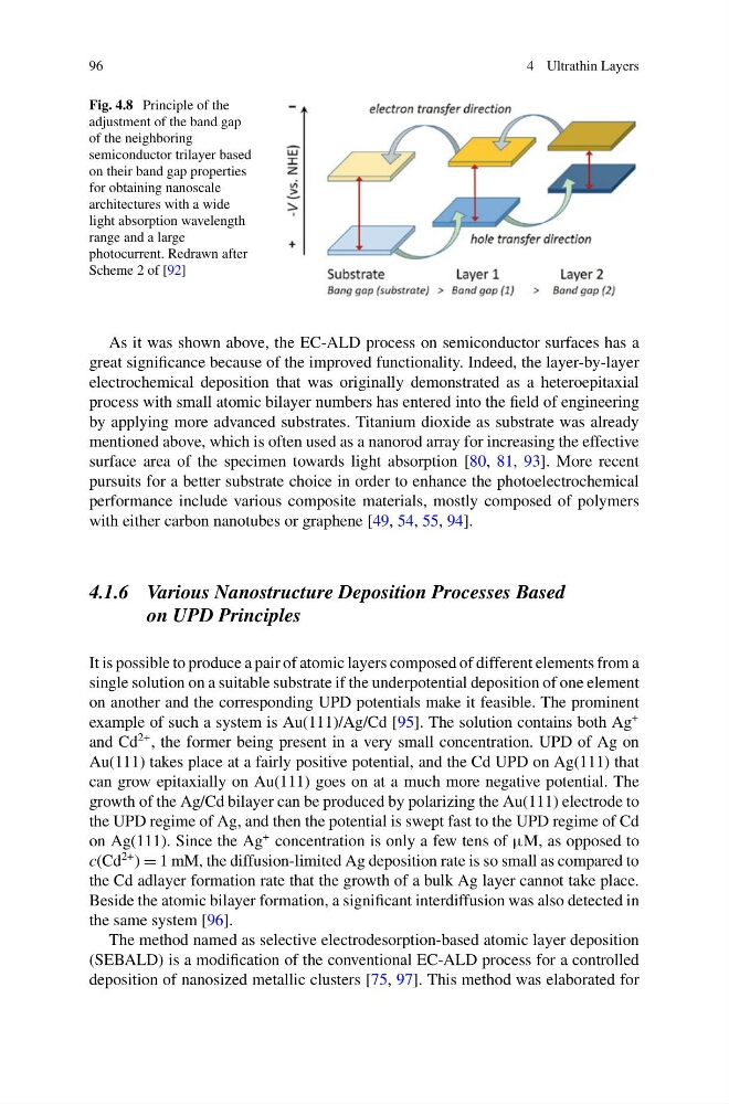
Fig. 4.8 Principle of the
adjustment of the band gap
of the neighboring
semiconductor trilayer based
on their band gap properties
for obtaining nanoscale
architectures with a wide
light absorption wavelength
range and a large
photocurrent. Redrawn after
Scheme 2 of [92]
As it was shown above, the EC-ALD process on semiconductor surfaces has a
great significance because of the improved functionality. Indeed, the layer-by-layer
electrochemical deposition that was originally demonstrated as a heteroepitaxial
process with small atomic bilayer numbers has entered into the field of engineering
by applying more advanced substrates. Titanium dioxide as substrate was already
mentioned above, which is often used as a nanorod array for increasing the effective
surface area of the specimen towards light absorption [80, 81, 93]. More recent
pursuits for a better substrate choice in order to enhance the photoelectrochemical
performance include various composite materials, mostly composed of polymers
with either carbon nanotubes or graphene [49, 54, 55, 94].
4.1.6 Various Nanostructure Deposition Processes Based
on UPD Principles
It is possible to produce a pair of atomic layers composed of different elements from a
single solution on a suitable substrate if the underpotential deposition of one element
on another and the corresponding UPD potentials make it feasible. The prominent
example of such a system is Au(111)/Ag/Cd [95]. The solution contains both Ag
+
and Cd
2+ , the former being present in a very small concentration. UPD of Ag on
Au(111) takes place at a fairly positive potential, and the Cd UPD on Ag(111) that
can grow epitaxially on Au(111) goes on at a much more negative potential. The
growth of the Ag/Cd bilayer can be produced by polarizing the Au(111) electrode to
the UPD regime of Ag, and then the potential is swept fast to the UPD regime of Cd
on Ag(111). Since the Ag
+ concentration is only a few tens of μM, as opposed to
c(Cd
2+ ) = 1 mM, the diffusion-limited Ag deposition rate is so small as compared to
the Cd adlayer formation rate that the growth of a bulk Ag layer cannot take place.
Beside the atomic bilayer formation, a significant interdiffusion was also detected in
the same system [96].
The method named as selective electrodesorption-based atomic layer deposition
(SEBALD) is a modification of the conventional EC-ALD process for a controlled
deposition of nanosized metallic clusters [75, 97]. This method was elaborated for
4 Ultrathin Layers
Fig. 4.8 Principle of the
adjustment of the band gap
of the neighboring
semiconductor trilayer based
on their band gap properties
for obtaining nanoscale
architectures with a wide
light absorption wavelength
range and a large
photocurrent. Redrawn after
Scheme 2 of [92]
As it was shown above, the EC-ALD process on semiconductor surfaces has a
great significance because of the improved functionality. Indeed, the layer-by-layer
electrochemical deposition that was originally demonstrated as a heteroepitaxial
process with small atomic bilayer numbers has entered into the field of engineering
by applying more advanced substrates. Titanium dioxide as substrate was already
mentioned above, which is often used as a nanorod array for increasing the effective
surface area of the specimen towards light absorption [80, 81, 93]. More recent
pursuits for a better substrate choice in order to enhance the photoelectrochemical
performance include various composite materials, mostly composed of polymers
with either carbon nanotubes or graphene [49, 54, 55, 94].
4.1.6 Various Nanostructure Deposition Processes Based
on UPD Principles
It is possible to produce a pair of atomic layers composed of different elements from a
single solution on a suitable substrate if the underpotential deposition of one element
on another and the corresponding UPD potentials make it feasible. The prominent
example of such a system is Au(111)/Ag/Cd [95]. The solution contains both Ag
+
and Cd
2+ , the former being present in a very small concentration. UPD of Ag on
Au(111) takes place at a fairly positive potential, and the Cd UPD on Ag(111) that
can grow epitaxially on Au(111) goes on at a much more negative potential. The
growth of the Ag/Cd bilayer can be produced by polarizing the Au(111) electrode to
the UPD regime of Ag, and then the potential is swept fast to the UPD regime of Cd
on Ag(111). Since the Ag
+ concentration is only a few tens of μM, as opposed to
c(Cd
2+ ) = 1 mM, the diffusion-limited Ag deposition rate is so small as compared to
the Cd adlayer formation rate that the growth of a bulk Ag layer cannot take place.
Beside the atomic bilayer formation, a significant interdiffusion was also detected in
the same system [96].
The method named as selective electrodesorption-based atomic layer deposition
(SEBALD) is a modification of the conventional EC-ALD process for a controlled
deposition of nanosized metallic clusters [75, 97]. This method was elaborated for