

4.1 Layer Preparation Methods Based Solely on UPD Processes
91
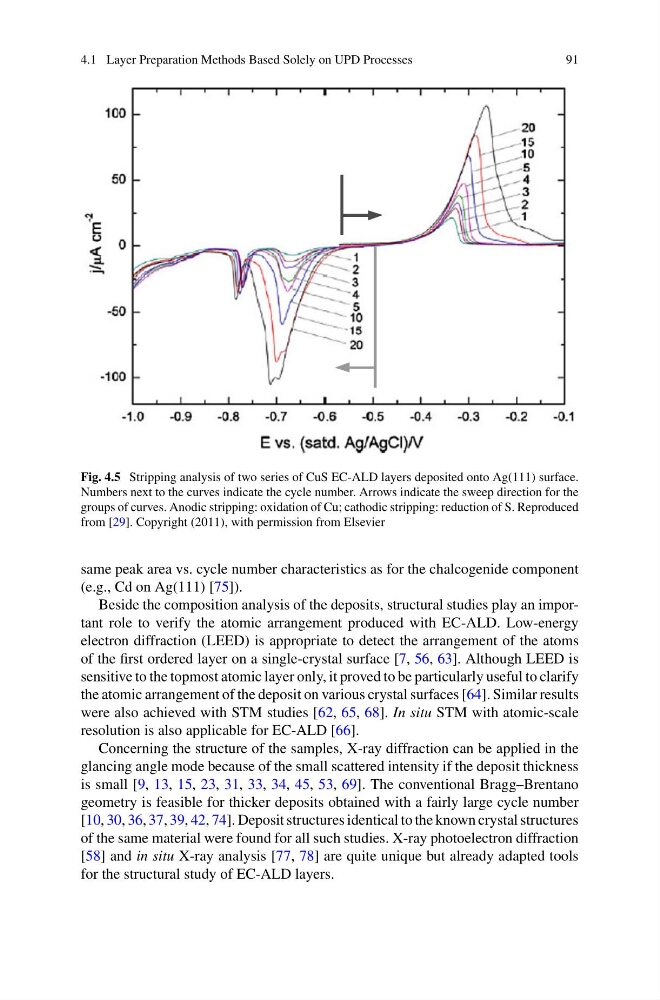
Fig. 4.5 Stripping analysis of two series of CuS EC-ALD layers deposited onto Ag(111) surface.
Numbers next to the curves indicate the cycle number. Arrows indicate the sweep direction for the
groups of curves. Anodic stripping: oxidation of Cu; cathodic stripping: reduction of S. Reproduced
from [29]. Copyright (2011), with permission from Elsevier
same peak area vs. cycle number characteristics as for the chalcogenide component
(e.g., Cd on Ag(111) [75]).
Beside the composition analysis of the deposits, structural studies play an important role to verify the atomic arrangement produced with EC-ALD. Low-energy
electron diffraction (LEED) is appropriate to detect the arrangement of the atoms
of the first ordered layer on a single-crystal surface [7, 56, 63]. Although LEED is
sensitive to the topmost atomic layer only, it proved to be particularly useful to clarify
the atomic arrangement of the deposit on various crystal surfaces [64]. Similar results
were also achieved with STM studies [62, 65, 68]. In situ STM with atomic-scale
resolution is also applicable for EC-ALD [66].
Concerning the structure of the samples, X-ray diffraction can be applied in the
glancing angle mode because of the small scattered intensity if the deposit thickness
is small [9, 13, 15, 23, 31, 33, 34, 45, 53, 69]. The conventional Bragg–Brentano
geometry is feasible for thicker deposits obtained with a fairly large cycle number
[10, 30, 36, 37, 39, 42, 74]. Deposit structures identical to the known crystal structures
of the same material were found for all such studies. X-ray photoelectron diffraction
[58] and in situ X-ray analysis [77, 78] are quite unique but already adapted tools
for the structural study of EC-ALD layers.
91
Fig. 4.5 Stripping analysis of two series of CuS EC-ALD layers deposited onto Ag(111) surface.
Numbers next to the curves indicate the cycle number. Arrows indicate the sweep direction for the
groups of curves. Anodic stripping: oxidation of Cu; cathodic stripping: reduction of S. Reproduced
from [29]. Copyright (2011), with permission from Elsevier
same peak area vs. cycle number characteristics as for the chalcogenide component
(e.g., Cd on Ag(111) [75]).
Beside the composition analysis of the deposits, structural studies play an important role to verify the atomic arrangement produced with EC-ALD. Low-energy
electron diffraction (LEED) is appropriate to detect the arrangement of the atoms
of the first ordered layer on a single-crystal surface [7, 56, 63]. Although LEED is
sensitive to the topmost atomic layer only, it proved to be particularly useful to clarify
the atomic arrangement of the deposit on various crystal surfaces [64]. Similar results
were also achieved with STM studies [62, 65, 68]. In situ STM with atomic-scale
resolution is also applicable for EC-ALD [66].
Concerning the structure of the samples, X-ray diffraction can be applied in the
glancing angle mode because of the small scattered intensity if the deposit thickness
is small [9, 13, 15, 23, 31, 33, 34, 45, 53, 69]. The conventional Bragg–Brentano
geometry is feasible for thicker deposits obtained with a fairly large cycle number
[10, 30, 36, 37, 39, 42, 74]. Deposit structures identical to the known crystal structures
of the same material were found for all such studies. X-ray photoelectron diffraction
[58] and in situ X-ray analysis [77, 78] are quite unique but already adapted tools
for the structural study of EC-ALD layers.