

84
4 Ultrathin Layers
the solution is changed, so that the surface layer is well conserved for the study of the
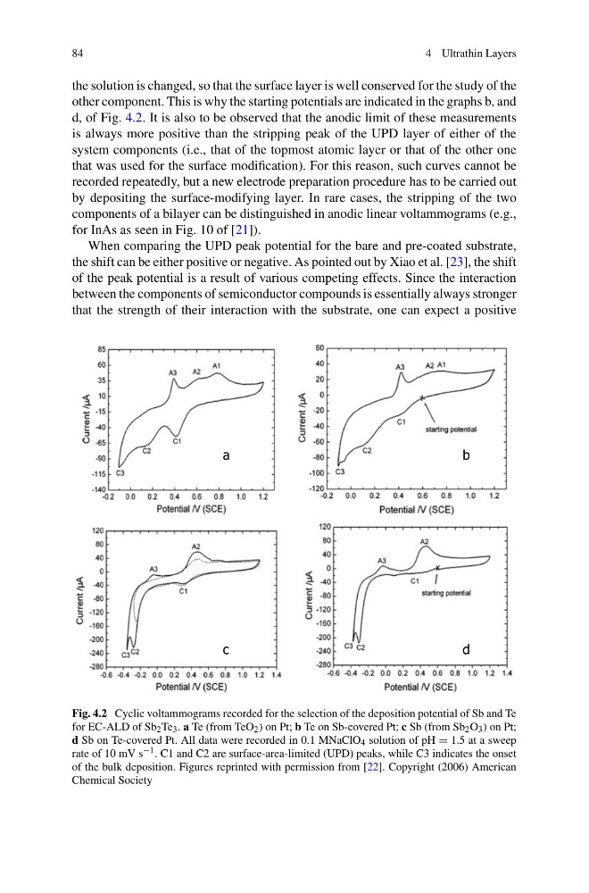
other component. This is why the starting potentials are indicated in the graphs b, and
d, of Fig. 4.2. It is also to be observed that the anodic limit of these measurements
is always more positive than the stripping peak of the UPD layer of either of the
system components (i.e., that of the topmost atomic layer or that of the other one
that was used for the surface modification). For this reason, such curves cannot be
recorded repeatedly, but a new electrode preparation procedure has to be carried out
by depositing the surface-modifying layer. In rare cases, the stripping of the two
components of a bilayer can be distinguished in anodic linear voltammograms (e.g.,
for InAs as seen in Fig. 10 of [21]).
When comparing the UPD peak potential for the bare and pre-coated substrate,
the shift can be either positive or negative. As pointed out by Xiao et al. [23], the shift
of the peak potential is a result of various competing effects. Since the interaction
between the components of semiconductor compounds is essentially always stronger
that the strength of their interaction with the substrate, one can expect a positive
a
b
c
d
Fig. 4.2 Cyclic voltammograms recorded for the selection of the deposition potential of Sb and Te
for EC-ALD of Sb 2 Te 3 . a Te (from TeO 2 ) on Pt; b Te on Sb-covered Pt; c Sb (from Sb 2 O 3 ) on Pt;
d Sb on Te-covered Pt. All data were recorded in 0.1 MNaClO 4 solution of pH = 1.5 at a sweep
rate of 10 mV s −1 . C1 and C2 are surface-area-limited (UPD) peaks, while C3 indicates the onset
of the bulk deposition. Figures reprinted with permission from [22]. Copyright (2006) American
Chemical Society
4 Ultrathin Layers
the solution is changed, so that the surface layer is well conserved for the study of the
other component. This is why the starting potentials are indicated in the graphs b, and
d, of Fig. 4.2. It is also to be observed that the anodic limit of these measurements
is always more positive than the stripping peak of the UPD layer of either of the
system components (i.e., that of the topmost atomic layer or that of the other one
that was used for the surface modification). For this reason, such curves cannot be
recorded repeatedly, but a new electrode preparation procedure has to be carried out
by depositing the surface-modifying layer. In rare cases, the stripping of the two
components of a bilayer can be distinguished in anodic linear voltammograms (e.g.,
for InAs as seen in Fig. 10 of [21]).
When comparing the UPD peak potential for the bare and pre-coated substrate,
the shift can be either positive or negative. As pointed out by Xiao et al. [23], the shift
of the peak potential is a result of various competing effects. Since the interaction
between the components of semiconductor compounds is essentially always stronger
that the strength of their interaction with the substrate, one can expect a positive
a
b
c
d
Fig. 4.2 Cyclic voltammograms recorded for the selection of the deposition potential of Sb and Te
for EC-ALD of Sb 2 Te 3 . a Te (from TeO 2 ) on Pt; b Te on Sb-covered Pt; c Sb (from Sb 2 O 3 ) on Pt;
d Sb on Te-covered Pt. All data were recorded in 0.1 MNaClO 4 solution of pH = 1.5 at a sweep
rate of 10 mV s −1 . C1 and C2 are surface-area-limited (UPD) peaks, while C3 indicates the onset
of the bulk deposition. Figures reprinted with permission from [22]. Copyright (2006) American
Chemical Society