

58
M. Hiramoto
(a)
NTCDA
5 mm
(b)
h +
ITO
e -
L = 0 μm
Hole Collection
Electrode
DBP
hν
h +
3
4
Lateral Electron Transport Crystal
(NTCDA)
e -
L =30 μm
L = 50 μm
L = 100 μm
Inter-electrode Distance (L)
(MoO 3 /Ag)
Electron Collection
Electrode
(Ag)
Starting point for electrons
DBP
(30 nm)
NTCDA
deposited film
(50 nm)
D/A
interface
(c)
NTCDA
DBP
Electron energy / eV
3.0
5.0
6.0
4.0
7.0
8.0
h +
e -
8.0
4.0
3.5
5.5
hν
LUMO
HOMO
1
2
L =20 μm
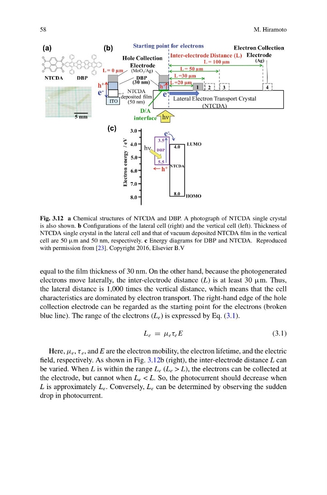
Fig. 3.12 a Chemical structures of NTCDA and DBP. A photograph of NTCDA single crystal
is also shown. b Configurations of the lateral cell (right) and the vertical cell (left). Thickness of
NTCDA single crystal in the lateral cell and that of vacuum deposited NTCDA film in the vertical
cell are 50 μm and 50 nm, respectively. c Energy diagrams for DBP and NTCDA. Reproduced
with permission from [23]. Copyright 2016, Elsevier B.V
equal to the film thickness of 30 nm. On the other hand, because the photogenerated
electrons move laterally, the inter-electrode distance (L) is at least 30 μm. Thus,
the lateral distance is 1,000 times the vertical distance, which means that the cell
characteristics are dominated by electron transport. The right-hand edge of the hole
collection electrode can be regarded as the starting point for the electrons (broken
blue line). The range of the electrons (L e ) is expressed by Eq. (3.1).
L e = μ e τ e E
(3.1)
Here, μ e , τ e , and E are the electron mobility, the electron lifetime, and the electric
field, respectively. As shown in Fig. 3.12b (right), the inter-electrode distance L can
be varied. When L is within the range L e (L e > L), the electrons can be collected at
the electrode, but cannot when L e < L. So, the photocurrent should decrease when
L is approximately L e . Conversely, L e can be determined by observing the sudden
drop in photocurrent.
M. Hiramoto
(a)
NTCDA
5 mm
(b)
h +
ITO
e -
L = 0 μm
Hole Collection
Electrode
DBP
hν
h +
3
4
Lateral Electron Transport Crystal
(NTCDA)
e -
L =30 μm
L = 50 μm
L = 100 μm
Inter-electrode Distance (L)
(MoO 3 /Ag)
Electron Collection
Electrode
(Ag)
Starting point for electrons
DBP
(30 nm)
NTCDA
deposited film
(50 nm)
D/A
interface
(c)
NTCDA
DBP
Electron energy / eV
3.0
5.0
6.0
4.0
7.0
8.0
h +
e -
8.0
4.0
3.5
5.5
hν
LUMO
HOMO
1
2
L =20 μm
Fig. 3.12 a Chemical structures of NTCDA and DBP. A photograph of NTCDA single crystal
is also shown. b Configurations of the lateral cell (right) and the vertical cell (left). Thickness of
NTCDA single crystal in the lateral cell and that of vacuum deposited NTCDA film in the vertical
cell are 50 μm and 50 nm, respectively. c Energy diagrams for DBP and NTCDA. Reproduced
with permission from [23]. Copyright 2016, Elsevier B.V
equal to the film thickness of 30 nm. On the other hand, because the photogenerated
electrons move laterally, the inter-electrode distance (L) is at least 30 μm. Thus,
the lateral distance is 1,000 times the vertical distance, which means that the cell
characteristics are dominated by electron transport. The right-hand edge of the hole
collection electrode can be regarded as the starting point for the electrons (broken
blue line). The range of the electrons (L e ) is expressed by Eq. (3.1).
L e = μ e τ e E
(3.1)
Here, μ e , τ e , and E are the electron mobility, the electron lifetime, and the electric
field, respectively. As shown in Fig. 3.12b (right), the inter-electrode distance L can
be varied. When L is within the range L e (L e > L), the electrons can be collected at
the electrode, but cannot when L e < L. So, the photocurrent should decrease when
L is approximately L e . Conversely, L e can be determined by observing the sudden
drop in photocurrent.