

244
M. Hiramoto
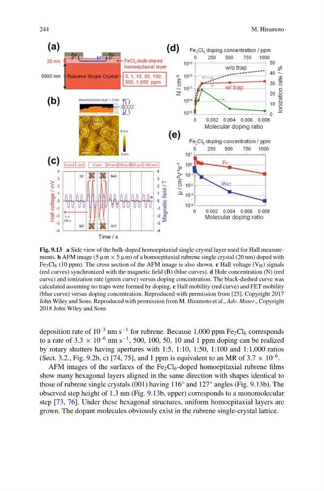
Fig. 9.13 a Side view of the bulk-doped homoepitaxial single-crystal layer used for Hall measurements. b AFM image (5 μm × 5 μm) of a homoepitaxial rubrene single crystal (20 nm) doped with
Fe 2 Cl 6 (10 ppm). The cross section of the AFM image is also shown. c Hall voltage (V H ) signals
(red curves) synchronized with the magnetic field (B) (blue curves). d Hole concentration (N) (red
curve) and ionization rate (green curve) versus doping concentration. The black-dashed curve was
calculated assuming no traps were formed by doping. e Hall mobility (red curve) and FET mobility
(blue curve) versus doping concentration. Reproduced with permission from [25]. Copyright 2017
John Wiley and Sons. Reproduced with permission from M. Hiramoto et al., Adv. Mater., Copyright
2018 John Wiley and Sons
deposition rate of 10
–3 nm s
−1 for rubrene. Because 1,000 ppm Fe 2 Cl 6 corresponds
to a rate of 3.3 × 10
–6 nm s
−1 , 500, 100, 50, 10 and 1 ppm doping can be realized
by rotary shutters having apertures with 1:5, 1:10, 1:50, 1:100 and 1:1,000 ratios
(Sect. 3.2., Fig. 9.2b, c) [74, 75], and 1 ppm is equivalent to an MR of 3.7 × 10
–6 .
AFM images of the surfaces of the Fe 2 Cl 6 -doped homoepitaxial rubrene films
show many hexagonal layers aligned in the same direction with shapes identical to
those of rubrene single crystals (001) having 116° and 127° angles (Fig. 9.13b). The
observed step height of 1.3 nm (Fig. 9.13b, upper) corresponds to a monomolecular
step [73, 76]. Under these hexagonal structures, uniform homoepitaxial layers are
grown. The dopant molecules obviously exist in the rubrene single-crystal lattice.
M. Hiramoto
Fig. 9.13 a Side view of the bulk-doped homoepitaxial single-crystal layer used for Hall measurements. b AFM image (5 μm × 5 μm) of a homoepitaxial rubrene single crystal (20 nm) doped with
Fe 2 Cl 6 (10 ppm). The cross section of the AFM image is also shown. c Hall voltage (V H ) signals
(red curves) synchronized with the magnetic field (B) (blue curves). d Hole concentration (N) (red
curve) and ionization rate (green curve) versus doping concentration. The black-dashed curve was
calculated assuming no traps were formed by doping. e Hall mobility (red curve) and FET mobility
(blue curve) versus doping concentration. Reproduced with permission from [25]. Copyright 2017
John Wiley and Sons. Reproduced with permission from M. Hiramoto et al., Adv. Mater., Copyright
2018 John Wiley and Sons
deposition rate of 10
–3 nm s
−1 for rubrene. Because 1,000 ppm Fe 2 Cl 6 corresponds
to a rate of 3.3 × 10
–6 nm s
−1 , 500, 100, 50, 10 and 1 ppm doping can be realized
by rotary shutters having apertures with 1:5, 1:10, 1:50, 1:100 and 1:1,000 ratios
(Sect. 3.2., Fig. 9.2b, c) [74, 75], and 1 ppm is equivalent to an MR of 3.7 × 10
–6 .
AFM images of the surfaces of the Fe 2 Cl 6 -doped homoepitaxial rubrene films
show many hexagonal layers aligned in the same direction with shapes identical to
those of rubrene single crystals (001) having 116° and 127° angles (Fig. 9.13b). The
observed step height of 1.3 nm (Fig. 9.13b, upper) corresponds to a monomolecular
step [73, 76]. Under these hexagonal structures, uniform homoepitaxial layers are
grown. The dopant molecules obviously exist in the rubrene single-crystal lattice.