

96
MIPS and NIPs. To improve contrast during high-resolution SEM imaging, the particles were stained with osmium tetroxide (OsO 4 ) vapor and embedded in epoxy
resin. The FIB/SEM technique facilitated the differentiation and visualization of the
distribution and connectivity of the pores and confirmed that their interconnectivity
in MIPs is significantly higher than in NIPs. TEM is also suitable for particle visualization. TEM measures a transmitted electron beam instead of the electrons
ejected from the surface and, to this end, the sample must be thin enough (~100 nm).
Additionally, as regards nanoparticle characterization In addition, with regard to the
characterization of NPs, some authors suggested dispersing them in ethanol, then
spreading them on carbon-coated copper grids, and finally, drying them at room
temperature (He et al. 2010; Lahcen et al. 2016; Cheng et al. 2019).
AFM is a type of scanning probe microcopy, which is also a powerful tool for
characterizing polymers. The AFM is suitable for studying the nucleation and
growth phenomena when high vacuum requirement in conventional electron microscopy prohibits the use of high temperatures (Hosier et al. 2004). The main advantage of AFM over TEM is the simplicity of sample preparation. AFM has been used
to study the surface topography of sensor chips without destruction of the surface,
supporting the profilometer data of the NP coating (Reimhult et al. 2008).
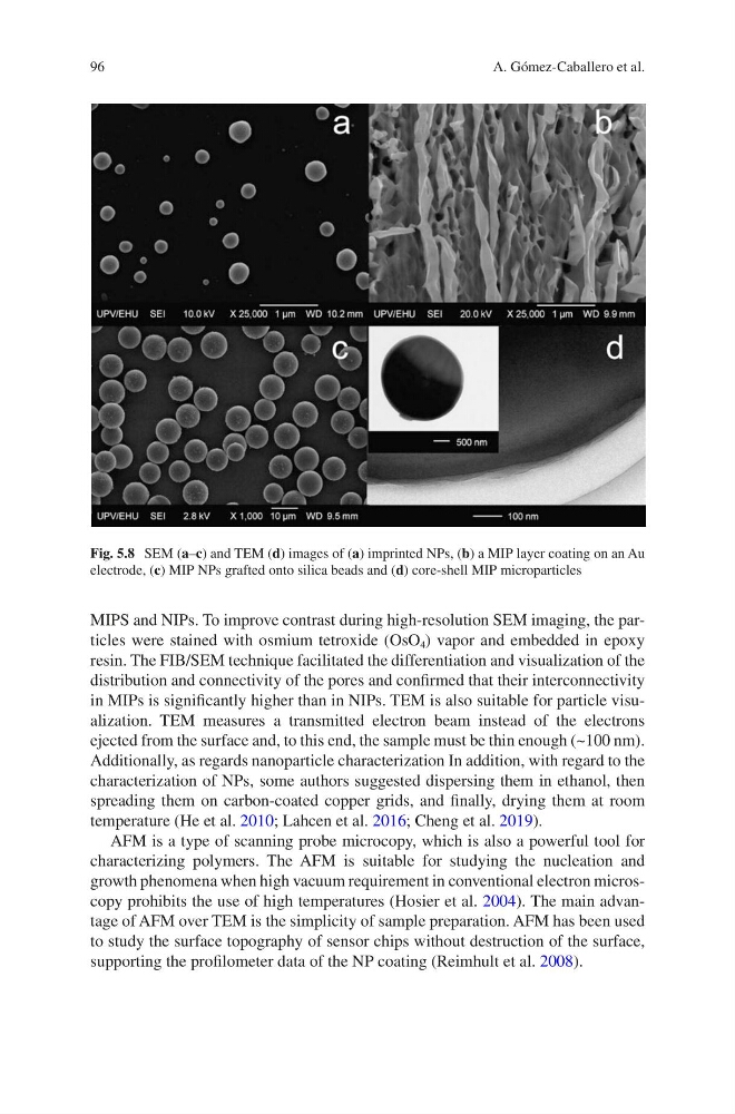
Fig. 5.8 SEM (a–c) and TEM (d) images of (a) imprinted NPs, (b) a MIP layer coating on an Au
electrode, (c) MIP NPs grafted onto silica beads and (d) core-shell MIP microparticles
A. Gómez-Caballero et al.
MIPS and NIPs. To improve contrast during high-resolution SEM imaging, the particles were stained with osmium tetroxide (OsO 4 ) vapor and embedded in epoxy
resin. The FIB/SEM technique facilitated the differentiation and visualization of the
distribution and connectivity of the pores and confirmed that their interconnectivity
in MIPs is significantly higher than in NIPs. TEM is also suitable for particle visualization. TEM measures a transmitted electron beam instead of the electrons
ejected from the surface and, to this end, the sample must be thin enough (~100 nm).
Additionally, as regards nanoparticle characterization In addition, with regard to the
characterization of NPs, some authors suggested dispersing them in ethanol, then
spreading them on carbon-coated copper grids, and finally, drying them at room
temperature (He et al. 2010; Lahcen et al. 2016; Cheng et al. 2019).
AFM is a type of scanning probe microcopy, which is also a powerful tool for
characterizing polymers. The AFM is suitable for studying the nucleation and
growth phenomena when high vacuum requirement in conventional electron microscopy prohibits the use of high temperatures (Hosier et al. 2004). The main advantage of AFM over TEM is the simplicity of sample preparation. AFM has been used
to study the surface topography of sensor chips without destruction of the surface,
supporting the profilometer data of the NP coating (Reimhult et al. 2008).
Fig. 5.8 SEM (a–c) and TEM (d) images of (a) imprinted NPs, (b) a MIP layer coating on an Au
electrode, (c) MIP NPs grafted onto silica beads and (d) core-shell MIP microparticles
A. Gómez-Caballero et al.