

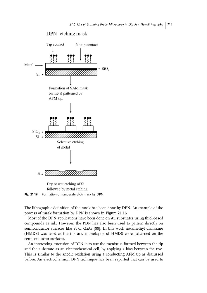
The lithographic definition of the mask has been done by DPN. An example of the
process of mask formation by DPN is shown in Figure 21.16.
Most of the DPN applications have been done on Au substrates using thiol-based
compounds as ink. However, the PDN has also been used to pattern directly on
semiconductor surfaces like Si or GaAs [88]. In this work hexamethyl disilazane
(HMDS) was used as the ink and monolayers of HMDS were patterned on the
semiconductor surfaces.
An interesting extension of DPN is to use the meniscus formed between the tip
and the substrate as an electrochemical cell, by applying a bias between the two.
This is similar to the anodic oxidation using a conducting AFM tip as discussed
before. An electrochemical DPN technique has been reported that can be used to
Fig. 21.16. Formation of nanoscale etch mask by DPN.
21.5 Use of Scanning Probe Microscopy in Dip Pen Nanolithography 715