

In recent years the anodic oxidation has been carried out by using pulsed mode
bias on the conducting AFM tip [68]. A room temperature single electron memory
was made by this method by growing TiO x on 2.5 nm Ti film grown on atomically
flat a-Al 2 O 3 . In the pulsed mode one uses a much lower voltage. In pulsed mode
while the positive bias of the substrate oxidizes the substrate the negative bias
neutralizes the positive space charge from the front end of the growing TiO x . The
single electron memory cells formed by the AFM anodic oxidation are around 10 to
15 nm in size and can store around 25 electrons. The single electron memory cell
showed hysteresis of a memory, even at room temperature.
The anodic oxide pattern of 100 nm dimension grown by SPM-based techniques
can be used as a mask that can be transferred to a substrate below. An anodized
alumina mask (produced by contact mode AFM on sputtered Al film) has been
used to transfer pattern on Si by using a combination of wet and reactive ion
etching. Anodic oxidation creates a protruding oxide pattern that can be etched.
The pattern can form a positive or negative mask depending on what is etched, the
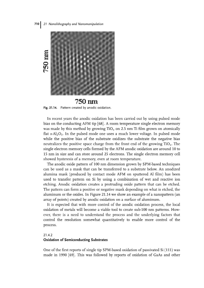
aluminum or the oxides. In Figure 21.14 we show an example of a nanopattern (an
array of points) created by anodic oxidation on a surface of aluminum.
It is expected that with more control of the anodic oxidation process, the local
oxidation of metals will become a viable tool to create sub-100 nm patterns. However, there is a need to understand the process and the underlying factors that
control the resolution somewhat quantitatively to enable more control of the
process.
21.4.2
Oxidation of Semiconducting Substrates
One of the first reports of single tip SPM-based oxidation of passivated Si (111) was
made in 1990 [69]. This was followed by reports of oxidation of GaAs and other
Fig. 21.14. Pattern created by anodic oxidation.
21 Nanolithography and Nanomanipulation
710