

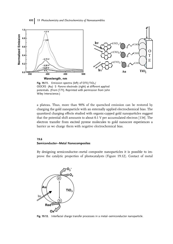
a plateau. Thus, more than 90% of the quenched emission can be restored by
charging the gold nanoparticle with an externally applied electrochemical bias. The
quantized charging effects studied with organic-capped gold nanoparticles suggest
that the potential shift amounts to about 0.1 V per accumulated electron [134]. The
electron transfer from excited pyrene molecules to gold nanocore experiences a
barrier as we charge them with negative electrochemical bias.
19.6
Semiconductor–Metal Nanocomposites
By designing semiconductor–metal composite nanoparticles it is possible to improve the catalytic properties of photocatalysts (Figure 19.12). Contact of metal
350
400
450
500
0.0
0.2
0.4
0.6
0.8
1.0
-1.2 V
- 1.0V
- 0.75 V
- 0.50 V
- 0.25 V
0 V
Normalized Emission
Wavelength, nm
O
T
E
TiO 2
2
e
h
h ‛
Au
−S
COO
–
−(CH2) n -S−S
COO
–
−(CH2) n -S−S
COO
–
−(CH2) n -SO
T
E
2
‛
−
–
−
−
–
−
–
− −
−S
–
−
n
−
–
−
–
− −
−S
–
−
–
−
-
−
-
350
400
450
500
0.0
0.2
0.4
0.6
0.8
1.0
-1.2 V
- 1.0V
- 0.75 V
- 0.50 V
- 0.25 V
0 V
Normalized Emission
Wavelength, nm
2
n
‛
−
–
−
−
–
−
−
–
−
-
2
n‛
–
−
– –
− −
–
−
– –
− −
−
–
−
–
− −
Fig. 19.11. Emission spectra (left) of OTE/TiO 2 /
OOCRSa(Au)aSaPyrene electrode (right) at different applied
potentials. (From [171]. Reprinted with permission from John
Wiley Interscience.)
hν
Au
TiO 2
e
h
Red
Ox
O 2
O 2
-
Fig. 19.12. Interfacial charge transfer processes in a metal–semiconductor nanoparticle.
19 Photochemistry and Electrochemistry of Nanoassemblies
632