

ried out using the same set of TB parameters listed in Table 11.1. This model describes the ab initio band structure better than any of the other TB models containing the s* orbital and excluding the next nearest neighbor (NNN) interactions.
Thus, this sp
3 d
5 -NNN model should be a good starting point for evaluating the
electronic structure of nanocrystals. With this model, the authors have calculated
the eigenvalue spectra of nanocrystals containing atoms ranging from 17 to 9527
[74, 75]. The dangling orbitals at the surface of the nanocrystals are passivated
using a layer of a higher band gap material. It is known from experiments that CdSe
surface can be passivated with ZnS overcoating [10]. We illustrate a realization of
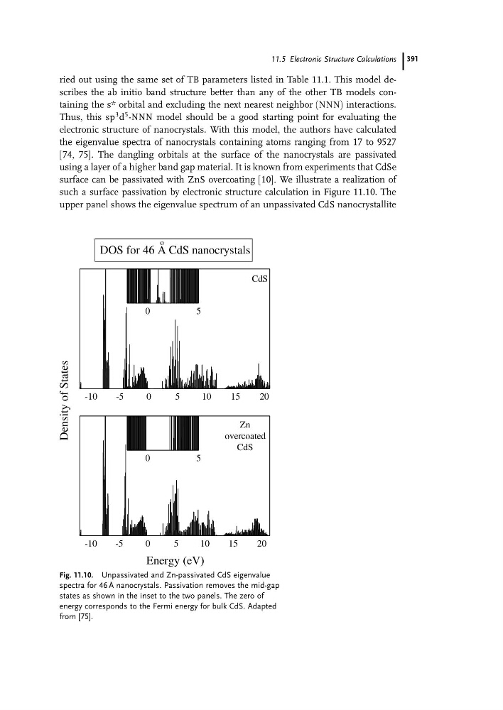
such a surface passivation by electronic structure calculation in Figure 11.10. The
upper panel shows the eigenvalue spectrum of an unpassivated CdS nanocrystallite
-10
-5
0
5
10
15
20
Density of States
Zn
overcoated
CdS
Energy (eV)
-10
-5
0
5
10
15
20
CdS
0
5
DOS for 46 A CdS nanocrystals
o
0
5
Fig. 11.10. Unpassivated and Zn-passivated CdS eigenvalue
spectra for 46 A ˚ nanocrystals. Passivation removes the mid-gap
states as shown in the inset to the two panels. The zero of
energy corresponds to the Fermi energy for bulk CdS. Adapted
from [75].
11.5 Electronic Structure Calculations 391
Thus, this sp
3 d
5 -NNN model should be a good starting point for evaluating the
electronic structure of nanocrystals. With this model, the authors have calculated
the eigenvalue spectra of nanocrystals containing atoms ranging from 17 to 9527
[74, 75]. The dangling orbitals at the surface of the nanocrystals are passivated
using a layer of a higher band gap material. It is known from experiments that CdSe
surface can be passivated with ZnS overcoating [10]. We illustrate a realization of
such a surface passivation by electronic structure calculation in Figure 11.10. The
upper panel shows the eigenvalue spectrum of an unpassivated CdS nanocrystallite
-10
-5
0
5
10
15
20
Density of States
Zn
overcoated
CdS
Energy (eV)
-10
-5
0
5
10
15
20
CdS
0
5
DOS for 46 A CdS nanocrystals
o
0
5
Fig. 11.10. Unpassivated and Zn-passivated CdS eigenvalue
spectra for 46 A ˚ nanocrystals. Passivation removes the mid-gap
states as shown in the inset to the two panels. The zero of
energy corresponds to the Fermi energy for bulk CdS. Adapted
from [75].
11.5 Electronic Structure Calculations 391