

nanotubes and nano-onions with plane spacings larger than those of graphite
(3.5–5.8 A ˚ ) were also formed. The latter were interpreted as hydrogenated carbon
nanotubes in which hydrogen atoms are bonded between graphitic layers forming
sp
3 bonding.
The TEM data indeed verifies that some carbon nanotubes (NTs) and nanoonions (NOs) were attached to the SiNWs (Figure 10.33). We believe that all the
NTs and NOs were formed on SiNW templates, since no NT/NO formation was
detected in the absence of SiNWs. Moreover, the NT and NO formation occurred
only when the oxide layer of the SiNWs was removed by HF dipping (H-terminated
SiNWs) but not on as-grown SiNWs with a SiO 2 sheath.
The template mechanism of the SiNWs is still unclear. We nevertheless believe
that the carbon nanostructures result from reactions between the SiH x species on
the SiNW surfaces. The substituents of the solvent material are eliminated by the
local heating caused by the sonication, giving rise to either C or CH units that wrap
around the SiNWs (templating effect). Further sonication causes the SiNWs to
shed off the NTs, refreshing the SiNW surfaces for additional templating of new
NTs. Prolonged sonication transforms all hydrogenated carbon NTs and NOs to
regular carbon structures: hydrogen free CNTs and CNOs.
10.7
Optical and Electrical Properties of SiNWs
10.7.1
Raman and PL of SiNWs [24]
The Raman spectrum of Si nanowires (Figure 10.34(a)) shows a broad and symmetric peak at 521 cm
À1 compared to that of a bulk single crystal Si. The peak
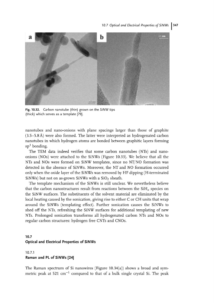
Fig. 10.32. Carbon nanotube (thin) grown on the SiNW tips
(thick) which serves as a template [79].
10.7 Optical and Electrical Properties of SiNWs 347
(3.5–5.8 A ˚ ) were also formed. The latter were interpreted as hydrogenated carbon
nanotubes in which hydrogen atoms are bonded between graphitic layers forming
sp
3 bonding.
The TEM data indeed verifies that some carbon nanotubes (NTs) and nanoonions (NOs) were attached to the SiNWs (Figure 10.33). We believe that all the
NTs and NOs were formed on SiNW templates, since no NT/NO formation was
detected in the absence of SiNWs. Moreover, the NT and NO formation occurred
only when the oxide layer of the SiNWs was removed by HF dipping (H-terminated
SiNWs) but not on as-grown SiNWs with a SiO 2 sheath.
The template mechanism of the SiNWs is still unclear. We nevertheless believe
that the carbon nanostructures result from reactions between the SiH x species on
the SiNW surfaces. The substituents of the solvent material are eliminated by the
local heating caused by the sonication, giving rise to either C or CH units that wrap
around the SiNWs (templating effect). Further sonication causes the SiNWs to
shed off the NTs, refreshing the SiNW surfaces for additional templating of new
NTs. Prolonged sonication transforms all hydrogenated carbon NTs and NOs to
regular carbon structures: hydrogen free CNTs and CNOs.
10.7
Optical and Electrical Properties of SiNWs
10.7.1
Raman and PL of SiNWs [24]
The Raman spectrum of Si nanowires (Figure 10.34(a)) shows a broad and symmetric peak at 521 cm
À1 compared to that of a bulk single crystal Si. The peak
Fig. 10.32. Carbon nanotube (thin) grown on the SiNW tips
(thick) which serves as a template [79].
10.7 Optical and Electrical Properties of SiNWs 347