

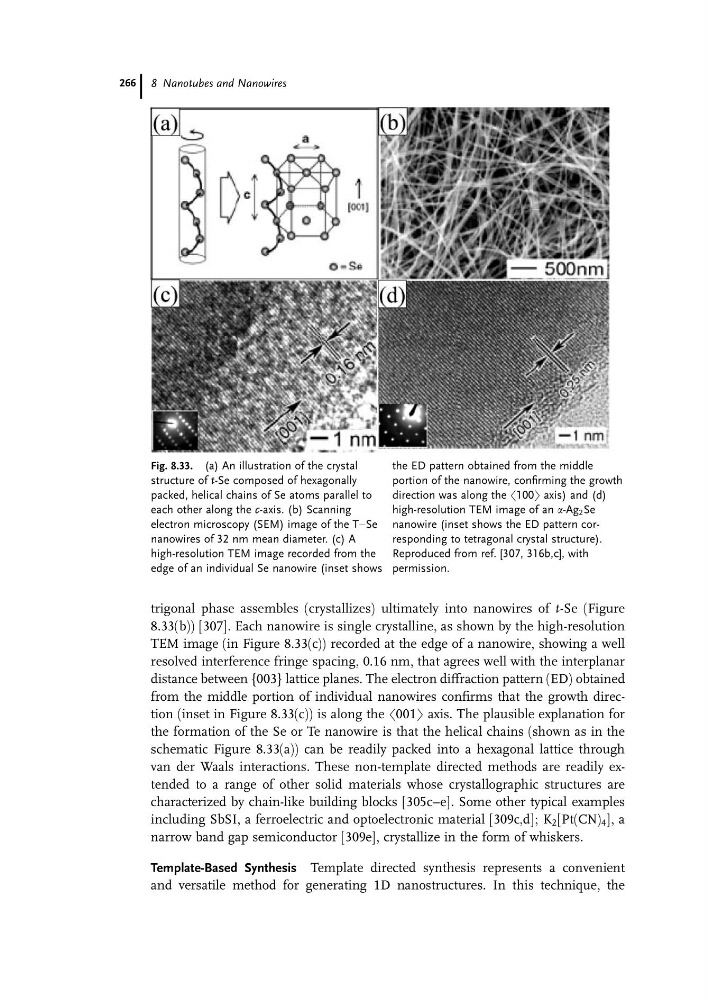
trigonal phase assembles (crystallizes) ultimately into nanowires of t-Se (Figure
8.33(b)) [307]. Each nanowire is single crystalline, as shown by the high-resolution
TEM image (in Figure 8.33(c)) recorded at the edge of a nanowire, showing a well
resolved interference fringe spacing, 0.16 nm, that agrees well with the interplanar
distance between {003} lattice planes. The electron diffraction pattern (ED) obtained
from the middle portion of individual nanowires confirms that the growth direction (inset in Figure 8.33(c)) is along the h001i axis. The plausible explanation for
the formation of the Se or Te nanowire is that the helical chains (shown as in the
schematic Figure 8.33(a)) can be readily packed into a hexagonal lattice through
van der Waals interactions. These non-template directed methods are readily extended to a range of other solid materials whose crystallographic structures are
characterized by chain-like building blocks [305c–e]. Some other typical examples
including SbSI, a ferroelectric and optoelectronic material [309c,d]; K 2 [Pt(CN) 4 ], a
narrow band gap semiconductor [309e], crystallize in the form of whiskers.
Template-Based Synthesis Template directed synthesis represents a convenient
and versatile method for generating 1D nanostructures. In this technique, the
Fig. 8.33. (a) An illustration of the crystal
structure of t-Se composed of hexagonally
packed, helical chains of Se atoms parallel to
each other along the c-axis. (b) Scanning
electron microscopy (SEM) image of the TaSe
nanowires of 32 nm mean diameter. (c) A
high-resolution TEM image recorded from the
edge of an individual Se nanowire (inset shows
the ED pattern obtained from the middle
portion of the nanowire, confirming the growth
direction was along the h100i axis) and (d)
high-resolution TEM image of an a-Ag 2 Se
nanowire (inset shows the ED pattern corresponding to tetragonal crystal structure).
Reproduced from ref. [307, 316b,c], with
permission.
8 Nanotubes and Nanowires
266
8.33(b)) [307]. Each nanowire is single crystalline, as shown by the high-resolution
TEM image (in Figure 8.33(c)) recorded at the edge of a nanowire, showing a well
resolved interference fringe spacing, 0.16 nm, that agrees well with the interplanar
distance between {003} lattice planes. The electron diffraction pattern (ED) obtained
from the middle portion of individual nanowires confirms that the growth direction (inset in Figure 8.33(c)) is along the h001i axis. The plausible explanation for
the formation of the Se or Te nanowire is that the helical chains (shown as in the
schematic Figure 8.33(a)) can be readily packed into a hexagonal lattice through
van der Waals interactions. These non-template directed methods are readily extended to a range of other solid materials whose crystallographic structures are
characterized by chain-like building blocks [305c–e]. Some other typical examples
including SbSI, a ferroelectric and optoelectronic material [309c,d]; K 2 [Pt(CN) 4 ], a
narrow band gap semiconductor [309e], crystallize in the form of whiskers.
Template-Based Synthesis Template directed synthesis represents a convenient
and versatile method for generating 1D nanostructures. In this technique, the
Fig. 8.33. (a) An illustration of the crystal
structure of t-Se composed of hexagonally
packed, helical chains of Se atoms parallel to
each other along the c-axis. (b) Scanning
electron microscopy (SEM) image of the TaSe
nanowires of 32 nm mean diameter. (c) A
high-resolution TEM image recorded from the
edge of an individual Se nanowire (inset shows
the ED pattern obtained from the middle
portion of the nanowire, confirming the growth
direction was along the h100i axis) and (d)
high-resolution TEM image of an a-Ag 2 Se
nanowire (inset shows the ED pattern corresponding to tetragonal crystal structure).
Reproduced from ref. [307, 316b,c], with
permission.
8 Nanotubes and Nanowires
266