

employs SWNT based lithography which offers sub-10 nm nanofabrication capabilities. In contrast to conventional electronic devices operating on the basis of
charge transport, spin-electronic devices operate upon the concept of spin transport.
Field Emission Industrial and academic research activity on electronic devices
has focused principally on using SWNTs and MWNTs as field emission electron
sources [185, 186] for flat panel displays [187], lamps [188], gas discharge tubes
providing surge protection [189], and X-rays [190]. A potential applied between a
carbon nanotube-coated surface and an anode produces high local fields, as a result
of the small radius of the nanofiber tip and the length of the nanofiber. These local
fields cause electrons to tunnel from the nanotube tip into the vacuum. Electric
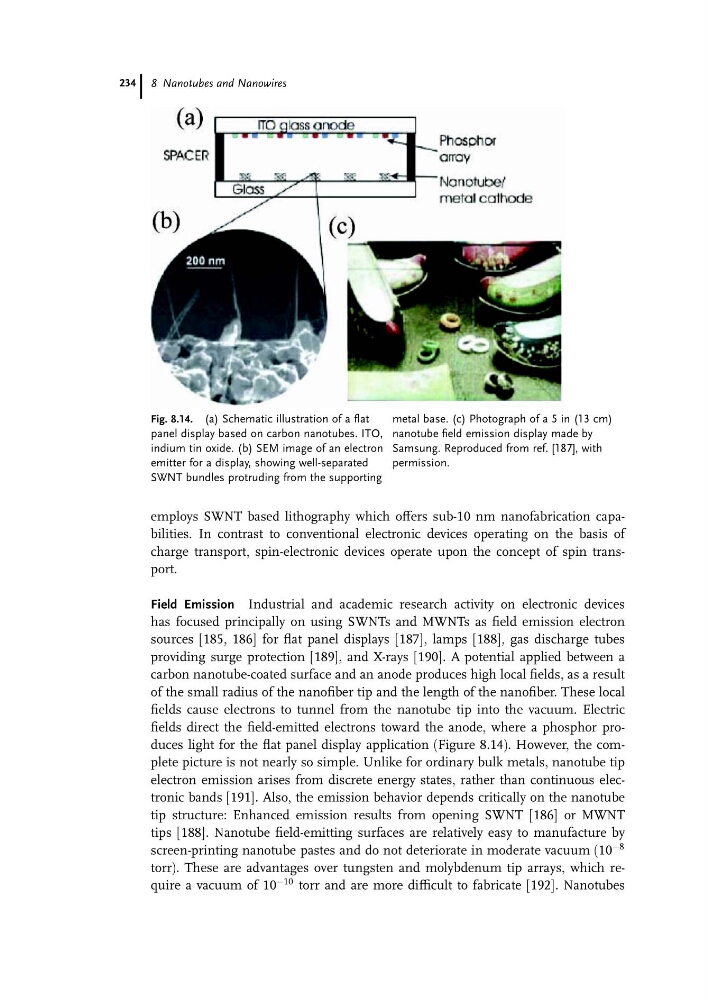
fields direct the field-emitted electrons toward the anode, where a phosphor produces light for the flat panel display application (Figure 8.14). However, the complete picture is not nearly so simple. Unlike for ordinary bulk metals, nanotube tip
electron emission arises from discrete energy states, rather than continuous electronic bands [191]. Also, the emission behavior depends critically on the nanotube
tip structure: Enhanced emission results from opening SWNT [186] or MWNT
tips [188]. Nanotube field-emitting surfaces are relatively easy to manufacture by
screen-printing nanotube pastes and do not deteriorate in moderate vacuum (10
À8
torr). These are advantages over tungsten and molybdenum tip arrays, which require a vacuum of 10
À10 torr and are more difficult to fabricate [192]. Nanotubes
Fig. 8.14. (a) Schematic illustration of a flat
panel display based on carbon nanotubes. ITO,
indium tin oxide. (b) SEM image of an electron
emitter for a display, showing well-separated
SWNT bundles protruding from the supporting
metal base. (c) Photograph of a 5 in (13 cm)
nanotube field emission display made by
Samsung. Reproduced from ref. [187], with
permission.
8 Nanotubes and Nanowires
234
charge transport, spin-electronic devices operate upon the concept of spin transport.
Field Emission Industrial and academic research activity on electronic devices
has focused principally on using SWNTs and MWNTs as field emission electron
sources [185, 186] for flat panel displays [187], lamps [188], gas discharge tubes
providing surge protection [189], and X-rays [190]. A potential applied between a
carbon nanotube-coated surface and an anode produces high local fields, as a result
of the small radius of the nanofiber tip and the length of the nanofiber. These local
fields cause electrons to tunnel from the nanotube tip into the vacuum. Electric
fields direct the field-emitted electrons toward the anode, where a phosphor produces light for the flat panel display application (Figure 8.14). However, the complete picture is not nearly so simple. Unlike for ordinary bulk metals, nanotube tip
electron emission arises from discrete energy states, rather than continuous electronic bands [191]. Also, the emission behavior depends critically on the nanotube
tip structure: Enhanced emission results from opening SWNT [186] or MWNT
tips [188]. Nanotube field-emitting surfaces are relatively easy to manufacture by
screen-printing nanotube pastes and do not deteriorate in moderate vacuum (10
À8
torr). These are advantages over tungsten and molybdenum tip arrays, which require a vacuum of 10
À10 torr and are more difficult to fabricate [192]. Nanotubes
Fig. 8.14. (a) Schematic illustration of a flat
panel display based on carbon nanotubes. ITO,
indium tin oxide. (b) SEM image of an electron
emitter for a display, showing well-separated
SWNT bundles protruding from the supporting
metal base. (c) Photograph of a 5 in (13 cm)
nanotube field emission display made by
Samsung. Reproduced from ref. [187], with
permission.
8 Nanotubes and Nanowires
234