

force microscope [162, 163]. A transistor assembled in this way may or may not
work, depending on whether the chosen nanotube is semiconducting or metallic,
over which the operator generally has no control. It is possible to selectively peel
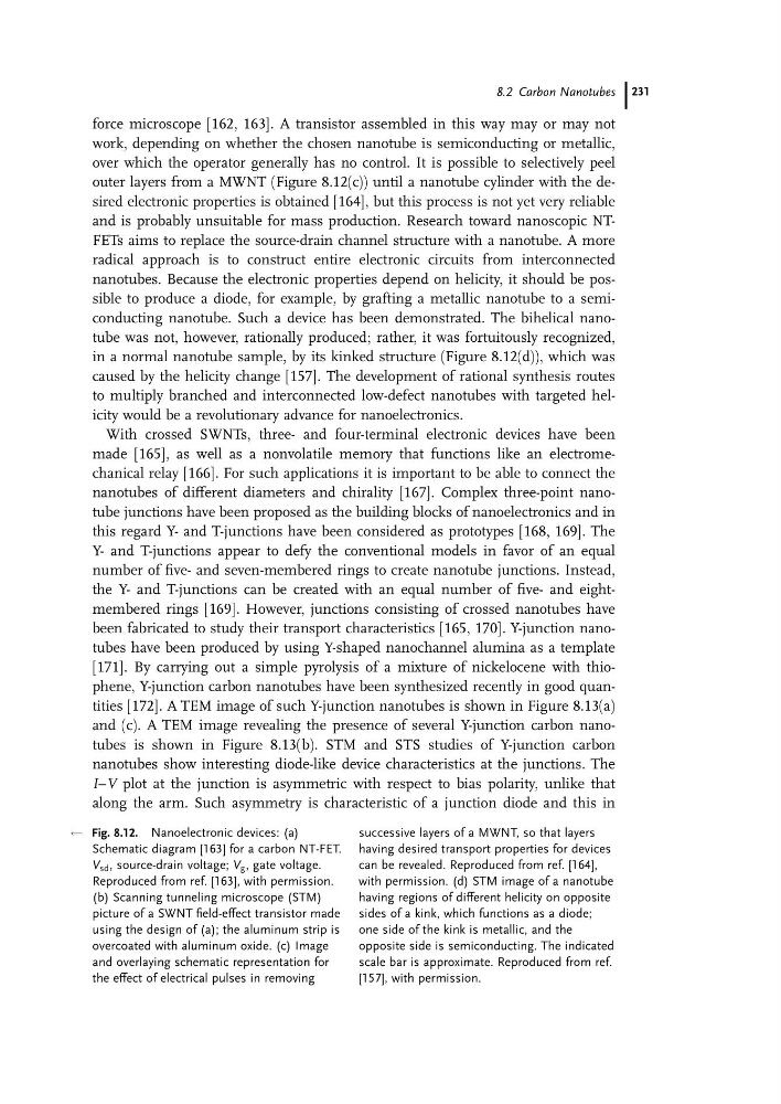
outer layers from a MWNT (Figure 8.12(c)) until a nanotube cylinder with the desired electronic properties is obtained [164], but this process is not yet very reliable
and is probably unsuitable for mass production. Research toward nanoscopic NTFETs aims to replace the source-drain channel structure with a nanotube. A more
radical approach is to construct entire electronic circuits from interconnected
nanotubes. Because the electronic properties depend on helicity, it should be possible to produce a diode, for example, by grafting a metallic nanotube to a semiconducting nanotube. Such a device has been demonstrated. The bihelical nanotube was not, however, rationally produced; rather, it was fortuitously recognized,
in a normal nanotube sample, by its kinked structure (Figure 8.12(d)), which was
caused by the helicity change [157]. The development of rational synthesis routes
to multiply branched and interconnected low-defect nanotubes with targeted helicity would be a revolutionary advance for nanoelectronics.
With crossed SWNTs, three- and four-terminal electronic devices have been
made [165], as well as a nonvolatile memory that functions like an electromechanical relay [166]. For such applications it is important to be able to connect the
nanotubes of different diameters and chirality [167]. Complex three-point nanotube junctions have been proposed as the building blocks of nanoelectronics and in
this regard Y- and T-junctions have been considered as prototypes [168, 169]. The
Y- and T-junctions appear to defy the conventional models in favor of an equal
number of five- and seven-membered rings to create nanotube junctions. Instead,
the Y- and T-junctions can be created with an equal number of five- and eightmembered rings [169]. However, junctions consisting of crossed nanotubes have
been fabricated to study their transport characteristics [165, 170]. Y-junction nanotubes have been produced by using Y-shaped nanochannel alumina as a template
[171]. By carrying out a simple pyrolysis of a mixture of nickelocene with thiophene, Y-junction carbon nanotubes have been synthesized recently in good quantities [172]. A TEM image of such Y-junction nanotubes is shown in Figure 8.13(a)
and (c). A TEM image revealing the presence of several Y-junction carbon nanotubes is shown in Figure 8.13(b). STM and STS studies of Y-junction carbon
nanotubes show interesting diode-like device characteristics at the junctions. The
I–V plot at the junction is asymmetric with respect to bias polarity, unlike that
along the arm. Such asymmetry is characteristic of a junction diode and this in
Fig. 8.12. Nanoelectronic devices: (a)
Schematic diagram [163] for a carbon NT-FET.
V sd , source-drain voltage; V g , gate voltage.
Reproduced from ref. [163], with permission.
(b) Scanning tunneling microscope (STM)
picture of a SWNT field-effect transistor made
using the design of (a); the aluminum strip is
overcoated with aluminum oxide. (c) Image
and overlaying schematic representation for
the effect of electrical pulses in removing
successive layers of a MWNT, so that layers
having desired transport properties for devices
can be revealed. Reproduced from ref. [164],
with permission. (d) STM image of a nanotube
having regions of different helicity on opposite
sides of a kink, which functions as a diode;
one side of the kink is metallic, and the
opposite side is semiconducting. The indicated
scale bar is approximate. Reproduced from ref.
[157], with permission.
8.2 Carbon Nanotubes 231
work, depending on whether the chosen nanotube is semiconducting or metallic,
over which the operator generally has no control. It is possible to selectively peel
outer layers from a MWNT (Figure 8.12(c)) until a nanotube cylinder with the desired electronic properties is obtained [164], but this process is not yet very reliable
and is probably unsuitable for mass production. Research toward nanoscopic NTFETs aims to replace the source-drain channel structure with a nanotube. A more
radical approach is to construct entire electronic circuits from interconnected
nanotubes. Because the electronic properties depend on helicity, it should be possible to produce a diode, for example, by grafting a metallic nanotube to a semiconducting nanotube. Such a device has been demonstrated. The bihelical nanotube was not, however, rationally produced; rather, it was fortuitously recognized,
in a normal nanotube sample, by its kinked structure (Figure 8.12(d)), which was
caused by the helicity change [157]. The development of rational synthesis routes
to multiply branched and interconnected low-defect nanotubes with targeted helicity would be a revolutionary advance for nanoelectronics.
With crossed SWNTs, three- and four-terminal electronic devices have been
made [165], as well as a nonvolatile memory that functions like an electromechanical relay [166]. For such applications it is important to be able to connect the
nanotubes of different diameters and chirality [167]. Complex three-point nanotube junctions have been proposed as the building blocks of nanoelectronics and in
this regard Y- and T-junctions have been considered as prototypes [168, 169]. The
Y- and T-junctions appear to defy the conventional models in favor of an equal
number of five- and seven-membered rings to create nanotube junctions. Instead,
the Y- and T-junctions can be created with an equal number of five- and eightmembered rings [169]. However, junctions consisting of crossed nanotubes have
been fabricated to study their transport characteristics [165, 170]. Y-junction nanotubes have been produced by using Y-shaped nanochannel alumina as a template
[171]. By carrying out a simple pyrolysis of a mixture of nickelocene with thiophene, Y-junction carbon nanotubes have been synthesized recently in good quantities [172]. A TEM image of such Y-junction nanotubes is shown in Figure 8.13(a)
and (c). A TEM image revealing the presence of several Y-junction carbon nanotubes is shown in Figure 8.13(b). STM and STS studies of Y-junction carbon
nanotubes show interesting diode-like device characteristics at the junctions. The
I–V plot at the junction is asymmetric with respect to bias polarity, unlike that
along the arm. Such asymmetry is characteristic of a junction diode and this in
Fig. 8.12. Nanoelectronic devices: (a)
Schematic diagram [163] for a carbon NT-FET.
V sd , source-drain voltage; V g , gate voltage.
Reproduced from ref. [163], with permission.
(b) Scanning tunneling microscope (STM)
picture of a SWNT field-effect transistor made
using the design of (a); the aluminum strip is
overcoated with aluminum oxide. (c) Image
and overlaying schematic representation for
the effect of electrical pulses in removing
successive layers of a MWNT, so that layers
having desired transport properties for devices
can be revealed. Reproduced from ref. [164],
with permission. (d) STM image of a nanotube
having regions of different helicity on opposite
sides of a kink, which functions as a diode;
one side of the kink is metallic, and the
opposite side is semiconducting. The indicated
scale bar is approximate. Reproduced from ref.
[157], with permission.
8.2 Carbon Nanotubes 231