

242
6 Photodetection Devices
discussions of semiconductor photodetectors and photodetection processes can be
found in the literature [1–12].
6.1 Operation of Photodiodes
6.1.1 The pin Photodetector
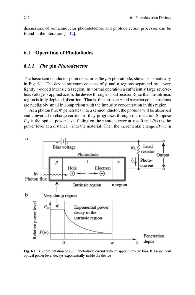
The basic semiconductor photodetector is the pin photodiode, shown schematically
in Fig. 6.1. The device structure consists of p and n regions separated by a very
lightly n-doped intrinsic (i) region. In normal operation a sufficiently large reversebias voltage is applied across the device through a load resistor R L so that the intrinsic
region is fully depleted of carriers. That is, the intrinsic n and p carrier concentrations
are negligibly small in comparison with the impurity concentration in this region.
As a photon flux penetrates into a semiconductor, the photons will be absorbed
and converted to charge carriers as they progresses through the material. Suppose
P in is the optical power level falling on the photodetector at x = 0 and P(x) is the
power level at a distance x into the material. Then the incremental change dP(x) in
Fig. 6.1 a Representation of a pin photodiode circuit with an applied reverse bias. b An incident
optical power level decays exponentially inside the device
6 Photodetection Devices
discussions of semiconductor photodetectors and photodetection processes can be
found in the literature [1–12].
6.1 Operation of Photodiodes
6.1.1 The pin Photodetector
The basic semiconductor photodetector is the pin photodiode, shown schematically
in Fig. 6.1. The device structure consists of p and n regions separated by a very
lightly n-doped intrinsic (i) region. In normal operation a sufficiently large reversebias voltage is applied across the device through a load resistor R L so that the intrinsic
region is fully depleted of carriers. That is, the intrinsic n and p carrier concentrations
are negligibly small in comparison with the impurity concentration in this region.
As a photon flux penetrates into a semiconductor, the photons will be absorbed
and converted to charge carriers as they progresses through the material. Suppose
P in is the optical power level falling on the photodetector at x = 0 and P(x) is the
power level at a distance x into the material. Then the incremental change dP(x) in
Fig. 6.1 a Representation of a pin photodiode circuit with an applied reverse bias. b An incident
optical power level decays exponentially inside the device