

90
V. L. Borblik
the structure are presented in Fig. 7. Characteristic feature of these distributions
is inhomogeneity of the field in the i-layer that sharply differs from the case of
planar p-i-n diode where electric field in the i-layer is homogeneous [21]. The field
inhomogeneity is especially strong when N A = N D or N A >> N D and diminishes
with thickening of the i-layer. In any case, the electric field is maximal near the
nanowire core.
It is of interest to study dependence of the electric field distributions on radial
position of the i-layer in the nanowire. Figure 8 represents such dependences for
three doping situations at the same thickness of the i-layer equal to 20 nm. It is
seen that as the i-layer moves away from a center of the nanowire, inhomogeneity
of the electric field distribution becomes more and more weak, i.e., the field goes to
homogeneous one inherent to planar p-i-n diode.
The dash lines in these figures demonstrate asymptotical confluence of both edge
values of the field in the i-layer when r 1 goes to infinity, i.e., the nanowire curvature
becomes ignorable. It is seen also that maximum electric field in the i-layer of the
nanowire proves to be higher than that in analogous planar diode at N A = N D and
N A >> N D and, on the contrary, is lower than that at N A << N D .
-0.4
-0.2
0.0
0.2
0.4
0.6
2.5x10
5
3.0x10
5
3.5x10
5
4.0x10
5
4.5x10
5
5.0x10
5
5.5x10
5
r 1 = 20 nm
r 2 - r 1 = 20 nm
N A = N D = 5x10
18 cm
-3
C, pF/cm 2
U, V
70
30
40
50
100
200
500
-0.4
-0.2
0.0
0.2
0.4
0.6
1.5x10
5
2.0x10
5
2.5x10
5
3.0x10
5
3.5x10
5
4.0x10
5
4.5x10
5
r 2 - r 1 = 20 nm
N A = 5x10
18 cm
-3 , N D = 5x10 17 cm -3
U, V
C,
pF/cm 2
r 1 = 20 nm
30
40
50
60
80
120
200
300
500
-0.6
-0.4
-0.2
0.0
0.2
0.4
0.6
5.0x10
4
1.0x10
5
1.5x10
5
2.0x10
5
2.5x10
5
r 2 - r 1 = 20 nm
N A = 5x10
17 cm
-3 , N D = 5x10 18 cm -3
C, pF/cm
2
500
300
200
150
120
U, V
r 1 = 60 nm
70
80
90
100
(a)
(b)
(c)
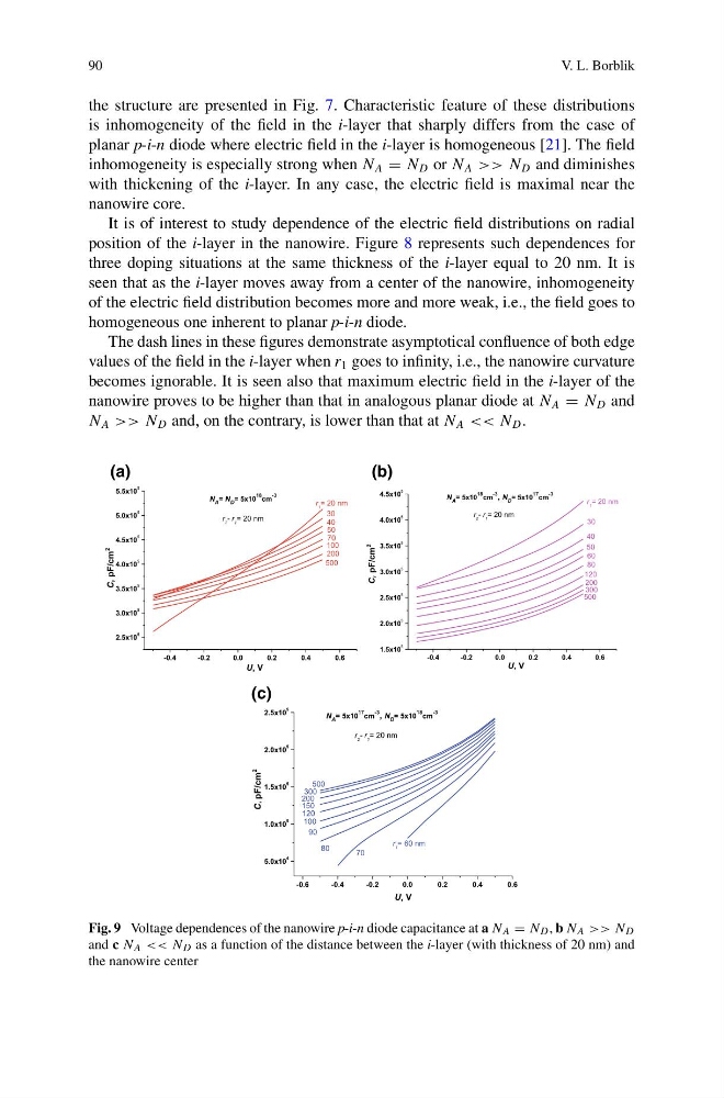
Fig. 9 Voltage dependences of the nanowire p-i-n diode capacitance at a N A = N D , b N A >> N D
and c N A << N D as a function of the distance between the i-layer (with thickness of 20 nm) and
the nanowire center
V. L. Borblik
the structure are presented in Fig. 7. Characteristic feature of these distributions
is inhomogeneity of the field in the i-layer that sharply differs from the case of
planar p-i-n diode where electric field in the i-layer is homogeneous [21]. The field
inhomogeneity is especially strong when N A = N D or N A >> N D and diminishes
with thickening of the i-layer. In any case, the electric field is maximal near the
nanowire core.
It is of interest to study dependence of the electric field distributions on radial
position of the i-layer in the nanowire. Figure 8 represents such dependences for
three doping situations at the same thickness of the i-layer equal to 20 nm. It is
seen that as the i-layer moves away from a center of the nanowire, inhomogeneity
of the electric field distribution becomes more and more weak, i.e., the field goes to
homogeneous one inherent to planar p-i-n diode.
The dash lines in these figures demonstrate asymptotical confluence of both edge
values of the field in the i-layer when r 1 goes to infinity, i.e., the nanowire curvature
becomes ignorable. It is seen also that maximum electric field in the i-layer of the
nanowire proves to be higher than that in analogous planar diode at N A = N D and
N A >> N D and, on the contrary, is lower than that at N A << N D .
-0.4
-0.2
0.0
0.2
0.4
0.6
2.5x10
5
3.0x10
5
3.5x10
5
4.0x10
5
4.5x10
5
5.0x10
5
5.5x10
5
r 1 = 20 nm
r 2 - r 1 = 20 nm
N A = N D = 5x10
18 cm
-3
C, pF/cm 2
U, V
70
30
40
50
100
200
500
-0.4
-0.2
0.0
0.2
0.4
0.6
1.5x10
5
2.0x10
5
2.5x10
5
3.0x10
5
3.5x10
5
4.0x10
5
4.5x10
5
r 2 - r 1 = 20 nm
N A = 5x10
18 cm
-3 , N D = 5x10 17 cm -3
U, V
C,
pF/cm 2
r 1 = 20 nm
30
40
50
60
80
120
200
300
500
-0.6
-0.4
-0.2
0.0
0.2
0.4
0.6
5.0x10
4
1.0x10
5
1.5x10
5
2.0x10
5
2.5x10
5
r 2 - r 1 = 20 nm
N A = 5x10
17 cm
-3 , N D = 5x10 18 cm -3
C, pF/cm
2
500
300
200
150
120
U, V
r 1 = 60 nm
70
80
90
100
(a)
(b)
(c)
Fig. 9 Voltage dependences of the nanowire p-i-n diode capacitance at a N A = N D , b N A >> N D
and c N A << N D as a function of the distance between the i-layer (with thickness of 20 nm) and
the nanowire center