

220
R. Singh et al.
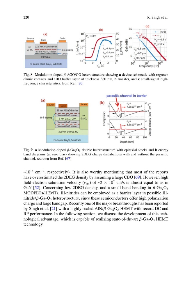
Fig. 8 Modulation-doped β-AGO/GO heterostructure showing a device schematic with regrown
ohmic contacts and UID buffer layer of thickness 360 nm, b transfer, and c small-signal highfrequency characteristics, from Ref. [20]
Fig. 9 a Modulation-doped β-Ga 2 O 3 double heterostructure with epitaxial stacks and b energy
band diagrams (at zero bias) showing 2DEG charge distributions with and without the parasitic
channel, redrawn from Ref. [67]
~10
13 cm
−2 , respectively). It is also worthy mentioning that most of the reports
have overestimated the 2DEG density by assuming a large CBO [69]. However, high
field-electron saturation velocity (v sat ) of ~2 × 10
7 cm/s is almost equal to as in
GaN [52]. Concerning low 2DEG density, and a small band bending in β-Ga 2 O 3
MODFETs/HEMTs, III-nitrides can be employed as a barrier layer in possible IIInitride/β-Ga 2 O 3 heterostructure, since these semiconductors offer high polarization
charge and large bandgap. Recently one of the major breakthroughs has been reported
by Singh et al. [21] with a highly scaled AlN/β-Ga 2 O 3 HEMT with record DC and
RF performance. In the following section, we discuss the development of this technological advantage, which is capable of realizing state-of-the-art β-Ga 2 O 3 HEMT
technology.
R. Singh et al.
Fig. 8 Modulation-doped β-AGO/GO heterostructure showing a device schematic with regrown
ohmic contacts and UID buffer layer of thickness 360 nm, b transfer, and c small-signal highfrequency characteristics, from Ref. [20]
Fig. 9 a Modulation-doped β-Ga 2 O 3 double heterostructure with epitaxial stacks and b energy
band diagrams (at zero bias) showing 2DEG charge distributions with and without the parasitic
channel, redrawn from Ref. [67]
~10
13 cm
−2 , respectively). It is also worthy mentioning that most of the reports
have overestimated the 2DEG density by assuming a large CBO [69]. However, high
field-electron saturation velocity (v sat ) of ~2 × 10
7 cm/s is almost equal to as in
GaN [52]. Concerning low 2DEG density, and a small band bending in β-Ga 2 O 3
MODFETs/HEMTs, III-nitrides can be employed as a barrier layer in possible IIInitride/β-Ga 2 O 3 heterostructure, since these semiconductors offer high polarization
charge and large bandgap. Recently one of the major breakthroughs has been reported
by Singh et al. [21] with a highly scaled AlN/β-Ga 2 O 3 HEMT with record DC and
RF performance. In the following section, we discuss the development of this technological advantage, which is capable of realizing state-of-the-art β-Ga 2 O 3 HEMT
technology.