

Ga 2 O 3 Based Heterostructure FETs (HFETs) for Microwave …
211
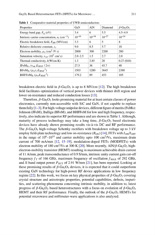
Table 1 Comparative material properties of UWB semiconductors
Properties
GaN
AlN
Diamond
β-Ga 2 O 3
Energy band gap, E g (eV)
3.4
6
5.5
4.5–4.9
Intrinsic carrier concentration, n i (cm −3 )
10 –10
10 –34
10 –27
10 –24
Electric breakdown field, E BR (MV/cm)
3.3
6
5
8
Relative dielectric constant, ε r
9.0
8.5
5.7
10
Electron mobility, μ n (cm 2 /V s)
2000
300
2200
200
Saturation velocity, v sat (10 7 cm/ s)
2.0–2.5
1.5
2.7
2.0
Thermal conductivity, k(W/cm K)
1.3
2.85
20
0.27 (010)
JFoM Si , (v sat E MAX / 2π)
27.5
36
45.7
40
BFoM Si (μ n ε r E MAX
3 )
1503
1280
3645
2380
BHFFoM Si (μ n E MAX
2 )
179.2
89
453
105
breakdown electric field in β-Ga 2 O 3 is up to 8 MV/cm [12]. The high breakdown
field facilitates optimization of vertical power devices with thinner drift region and
lower on-resistance and reduced conduction losses [13].
Therefore, β-Ga 2 O 3 looks promising material for at least certain classes of power
electronics, currently non-accessible with SiC and GaN, if not capable to replace
them fully [1–3]. For high-voltage unipolar devices, different figure of merits (FoMs):
Johnson (JFoM), Balliga (BFoM), and BHFFoM for low and high frequency, respectively, also indicate its superior RF performance and are shown in Table 1. Although,
maturity of process technology may take a long time, β-Ga 2 O 3 based electronic
devices have already shown promising results vis-à-vis DC and RF performance.
The β-Ga 2 O 3 high-voltage Schottky rectifiers with breakdown voltage up to 3 kV
employ field-plate technology and low on-resistance (R ON ) [14], FETs with I ON /I OFF
in the range of 10
6 –10
10 and carrier mobility upto 100 cm
2 /Vs, maximum drain
current of 700 mA/mm [12, 15–19], modulation-doped FETs (MODFETs) with
electron mobility of 180 cm
2 /Vs at 300 K [20]. More recently, AlN/β-Ga 2 O 3 highelectron-mobility transistor (HEMT) resulting in maximum achievable drain current
of 11 A/mm, peak transconductance of 0.9 S/mm, intrinsic unity current gain cut-off
frequency f T of 166 GHz, maximum frequency of oscillation f MAX of 292 GHz,
and X-band output power P OUT of 2.91 W/mm [21], has been reported. Looking at
these promising results of β-Ga 2 O 3 devices, it is expected that it could outperform
existing GaN technology for high-power RF device applications in low frequency
regime [22]. In this work, we focus on key physical properties of β-Ga 2 O 3 covering
crystal structure and anisotropic properties, potential capabilities, defects, impurities, and scattering phenomena concerning intrinsic mobility, in addition to, latest
progress of β-Ga 2 O 3 based heterostructures with a focus on evolution of β-Ga 2 O 3
HEMT and their RF performance. Finally, the outlook of the β-Ga 2 O 3 HEMTs for
potential microwave and millimeter-wave applications is also analyzed.
211
Table 1 Comparative material properties of UWB semiconductors
Properties
GaN
AlN
Diamond
β-Ga 2 O 3
Energy band gap, E g (eV)
3.4
6
5.5
4.5–4.9
Intrinsic carrier concentration, n i (cm −3 )
10 –10
10 –34
10 –27
10 –24
Electric breakdown field, E BR (MV/cm)
3.3
6
5
8
Relative dielectric constant, ε r
9.0
8.5
5.7
10
Electron mobility, μ n (cm 2 /V s)
2000
300
2200
200
Saturation velocity, v sat (10 7 cm/ s)
2.0–2.5
1.5
2.7
2.0
Thermal conductivity, k(W/cm K)
1.3
2.85
20
0.27 (010)
JFoM Si , (v sat E MAX / 2π)
27.5
36
45.7
40
BFoM Si (μ n ε r E MAX
3 )
1503
1280
3645
2380
BHFFoM Si (μ n E MAX
2 )
179.2
89
453
105
breakdown electric field in β-Ga 2 O 3 is up to 8 MV/cm [12]. The high breakdown
field facilitates optimization of vertical power devices with thinner drift region and
lower on-resistance and reduced conduction losses [13].
Therefore, β-Ga 2 O 3 looks promising material for at least certain classes of power
electronics, currently non-accessible with SiC and GaN, if not capable to replace
them fully [1–3]. For high-voltage unipolar devices, different figure of merits (FoMs):
Johnson (JFoM), Balliga (BFoM), and BHFFoM for low and high frequency, respectively, also indicate its superior RF performance and are shown in Table 1. Although,
maturity of process technology may take a long time, β-Ga 2 O 3 based electronic
devices have already shown promising results vis-à-vis DC and RF performance.
The β-Ga 2 O 3 high-voltage Schottky rectifiers with breakdown voltage up to 3 kV
employ field-plate technology and low on-resistance (R ON ) [14], FETs with I ON /I OFF
in the range of 10
6 –10
10 and carrier mobility upto 100 cm
2 /Vs, maximum drain
current of 700 mA/mm [12, 15–19], modulation-doped FETs (MODFETs) with
electron mobility of 180 cm
2 /Vs at 300 K [20]. More recently, AlN/β-Ga 2 O 3 highelectron-mobility transistor (HEMT) resulting in maximum achievable drain current
of 11 A/mm, peak transconductance of 0.9 S/mm, intrinsic unity current gain cut-off
frequency f T of 166 GHz, maximum frequency of oscillation f MAX of 292 GHz,
and X-band output power P OUT of 2.91 W/mm [21], has been reported. Looking at
these promising results of β-Ga 2 O 3 devices, it is expected that it could outperform
existing GaN technology for high-power RF device applications in low frequency
regime [22]. In this work, we focus on key physical properties of β-Ga 2 O 3 covering
crystal structure and anisotropic properties, potential capabilities, defects, impurities, and scattering phenomena concerning intrinsic mobility, in addition to, latest
progress of β-Ga 2 O 3 based heterostructures with a focus on evolution of β-Ga 2 O 3
HEMT and their RF performance. Finally, the outlook of the β-Ga 2 O 3 HEMTs for
potential microwave and millimeter-wave applications is also analyzed.