

All Optical Universal Logic TAND Gate Using a Single …
171
0.0 0.1 0.2 0.3 0.4 0.5 0.6 0.7 0.8 0.9 1.0 1.1
0.05
0.10
0.15
0.20
0.25
0.30
0.35
AM (dB)
Control Power (mW)
AM
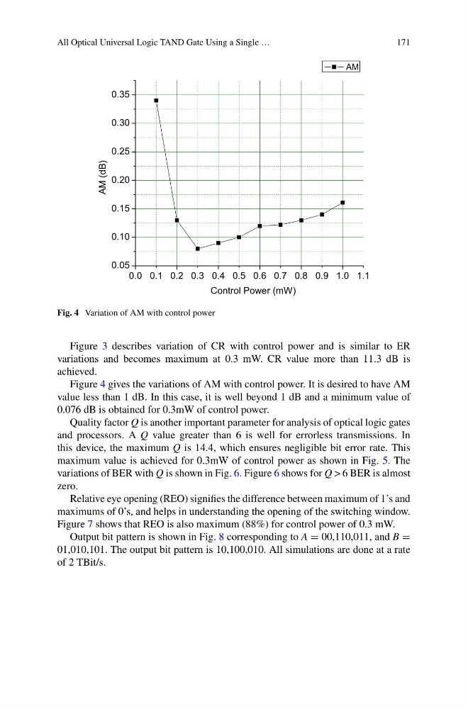
Fig. 4 Variation of AM with control power
Figure 3 describes variation of CR with control power and is similar to ER
variations and becomes maximum at 0.3 mW. CR value more than 11.3 dB is
achieved.
Figure 4 gives the variations of AM with control power. It is desired to have AM
value less than 1 dB. In this case, it is well beyond 1 dB and a minimum value of
0.076 dB is obtained for 0.3mW of control power.
Quality factor Q is another important parameter for analysis of optical logic gates
and processors. A Q value greater than 6 is well for errorless transmissions. In
this device, the maximum Q is 14.4, which ensures negligible bit error rate. This
maximum value is achieved for 0.3mW of control power as shown in Fig. 5. The
variations of BER with Q is shown in Fig. 6. Figure 6 shows for Q > 6 BER is almost
zero.
Relative eye opening (REO) signifies the difference between maximum of 1’s and
maximums of 0’s, and helps in understanding the opening of the switching window.
Figure 7 shows that REO is also maximum (88%) for control power of 0.3 mW.
Output bit pattern is shown in Fig. 8 corresponding to A = 00,110,011, and B =
01,010,101. The output bit pattern is 10,100,010. All simulations are done at a rate
of 2 TBit/s.
171
0.0 0.1 0.2 0.3 0.4 0.5 0.6 0.7 0.8 0.9 1.0 1.1
0.05
0.10
0.15
0.20
0.25
0.30
0.35
AM (dB)
Control Power (mW)
AM
Fig. 4 Variation of AM with control power
Figure 3 describes variation of CR with control power and is similar to ER
variations and becomes maximum at 0.3 mW. CR value more than 11.3 dB is
achieved.
Figure 4 gives the variations of AM with control power. It is desired to have AM
value less than 1 dB. In this case, it is well beyond 1 dB and a minimum value of
0.076 dB is obtained for 0.3mW of control power.
Quality factor Q is another important parameter for analysis of optical logic gates
and processors. A Q value greater than 6 is well for errorless transmissions. In
this device, the maximum Q is 14.4, which ensures negligible bit error rate. This
maximum value is achieved for 0.3mW of control power as shown in Fig. 5. The
variations of BER with Q is shown in Fig. 6. Figure 6 shows for Q > 6 BER is almost
zero.
Relative eye opening (REO) signifies the difference between maximum of 1’s and
maximums of 0’s, and helps in understanding the opening of the switching window.
Figure 7 shows that REO is also maximum (88%) for control power of 0.3 mW.
Output bit pattern is shown in Fig. 8 corresponding to A = 00,110,011, and B =
01,010,101. The output bit pattern is 10,100,010. All simulations are done at a rate
of 2 TBit/s.