

58
V. P. Drachev et al.
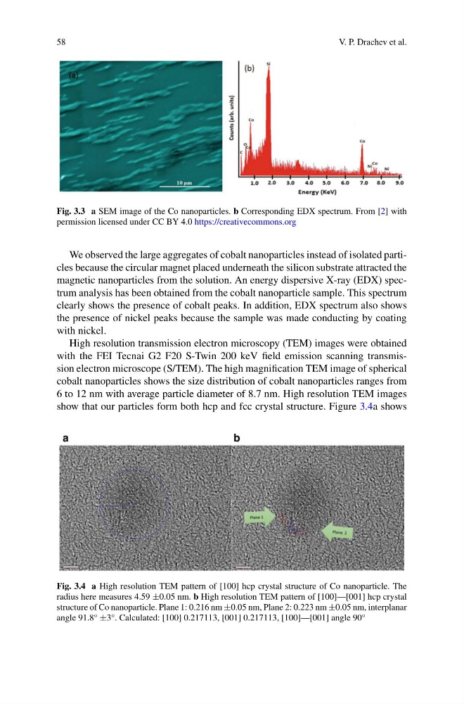
Fig. 3.3 a SEM image of the Co nanoparticles. b Corresponding EDX spectrum. From [2] with
permission licensed under CC BY 4.0 https://creativecommons.org
We observed the large aggregates of cobalt nanoparticles instead of isolated particles because the circular magnet placed underneath the silicon substrate attracted the
magnetic nanoparticles from the solution. An energy dispersive X-ray (EDX) spectrum analysis has been obtained from the cobalt nanoparticle sample. This spectrum
clearly shows the presence of cobalt peaks. In addition, EDX spectrum also shows
the presence of nickel peaks because the sample was made conducting by coating
with nickel.
High resolution transmission electron microscopy (TEM) images were obtained
with the FEI Tecnai G2 F20 S-Twin 200 keV field emission scanning transmission electron microscope (S/TEM). The high magnification TEM image of spherical
cobalt nanoparticles shows the size distribution of cobalt nanoparticles ranges from
6 to 12 nm with average particle diameter of 8.7 nm. High resolution TEM images
show that our particles form both hcp and fcc crystal structure. Figure 3.4a shows
Fig. 3.4 a High resolution TEM pattern of [100] hcp crystal structure of Co nanoparticle. The
radius here measures 4.59 ±0.05 nm. b High resolution TEM pattern of [100]—[001] hcp crystal
structure of Co nanoparticle. Plane 1: 0.216 nm ±0.05 nm, Plane 2: 0.223 nm ±0.05 nm, interplanar
angle 91.8° ±3°. Calculated: [100] 0.217113, [001] 0.217113, [100]—[001] angle 90°
V. P. Drachev et al.
Fig. 3.3 a SEM image of the Co nanoparticles. b Corresponding EDX spectrum. From [2] with
permission licensed under CC BY 4.0 https://creativecommons.org
We observed the large aggregates of cobalt nanoparticles instead of isolated particles because the circular magnet placed underneath the silicon substrate attracted the
magnetic nanoparticles from the solution. An energy dispersive X-ray (EDX) spectrum analysis has been obtained from the cobalt nanoparticle sample. This spectrum
clearly shows the presence of cobalt peaks. In addition, EDX spectrum also shows
the presence of nickel peaks because the sample was made conducting by coating
with nickel.
High resolution transmission electron microscopy (TEM) images were obtained
with the FEI Tecnai G2 F20 S-Twin 200 keV field emission scanning transmission electron microscope (S/TEM). The high magnification TEM image of spherical
cobalt nanoparticles shows the size distribution of cobalt nanoparticles ranges from
6 to 12 nm with average particle diameter of 8.7 nm. High resolution TEM images
show that our particles form both hcp and fcc crystal structure. Figure 3.4a shows
Fig. 3.4 a High resolution TEM pattern of [100] hcp crystal structure of Co nanoparticle. The
radius here measures 4.59 ±0.05 nm. b High resolution TEM pattern of [100]—[001] hcp crystal
structure of Co nanoparticle. Plane 1: 0.216 nm ±0.05 nm, Plane 2: 0.223 nm ±0.05 nm, interplanar
angle 91.8° ±3°. Calculated: [100] 0.217113, [001] 0.217113, [100]—[001] angle 90°