

10 Realization of Artificial Chirality in Micro-/Nano-Scale …
243
10.2 Chirality at the Micrometer-Scale or Higher:
Top-Down Approach
This chapter will introduce chiral plasmonic structures and their realization in
micrometer-scale or beyond by using top-down fabrication. Artificial microscale
structures generally interact with electromagnetic (EM) waves of 1 μm or more. The
wavelength range (λ > 1.0 μm) includes infrared and microwave regions; they can
be utilized for thermal detectors, light detection and ranging (LiDAR) devices, shortrange wireless communication antenna, and spectroscopy. With these applications in
mind, chiral plasmonic structures have been demonstrated from 1 μm size structures
to millimeter-scale chiral ones. In this subchapter, their fabrication methods will be
categorized by scales of artificial structures sizes; brief descriptions of chiroptical
phenomena will be added.
10.2.1 Direct Laser Writing
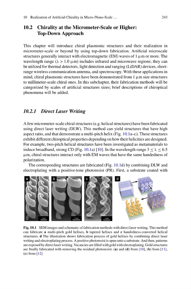
A few micrometer-scale chiral structures (e.g. helical structures) have been fabricated
using direct laser writing (DLW). This method can yield structures that have high
aspect ratio, and that demonstrate a multi-pitch helix (Fig. 10.1a–c). These structures
exhibit different chiroptical properties depending on how their helicities are designed.
For example, two-pitch helical structures have been investigated as metamaterials to
induce broadband, strong CD (Fig. 10.1a) [10]. In the wavelength range 3 ≤ λ ≤ 6.5
μm, chiral structures interact only with EM waves that have the same handedness of
polarization.
The corresponding structures are fabricated (Fig. 10.1d) by combining DLW and
electroplating with a positive-tone photoresist (PR). First, a substrate coated with
Fig. 10.1 SEM images and schematic of fabrication methods with direct laser writing. This method
can fabricate a multi-pitch gold helixes, b tapered helixes and c handedness-converted helical
structures. d The illustration shows fabrication process of gold helixes by combining direct laser
writing and electroplating process. A positive photoresist is spun onto a substrate. And then, patterns
are exposed by direct laser writing. Vacancies are filled with gold with electroplating. Gold structures
are finally fabricated with removing the residual photoresist. (a) and (d) from [10], (b) from [11],
(c) from [12]
243
10.2 Chirality at the Micrometer-Scale or Higher:
Top-Down Approach
This chapter will introduce chiral plasmonic structures and their realization in
micrometer-scale or beyond by using top-down fabrication. Artificial microscale
structures generally interact with electromagnetic (EM) waves of 1 μm or more. The
wavelength range (λ > 1.0 μm) includes infrared and microwave regions; they can
be utilized for thermal detectors, light detection and ranging (LiDAR) devices, shortrange wireless communication antenna, and spectroscopy. With these applications in
mind, chiral plasmonic structures have been demonstrated from 1 μm size structures
to millimeter-scale chiral ones. In this subchapter, their fabrication methods will be
categorized by scales of artificial structures sizes; brief descriptions of chiroptical
phenomena will be added.
10.2.1 Direct Laser Writing
A few micrometer-scale chiral structures (e.g. helical structures) have been fabricated
using direct laser writing (DLW). This method can yield structures that have high
aspect ratio, and that demonstrate a multi-pitch helix (Fig. 10.1a–c). These structures
exhibit different chiroptical properties depending on how their helicities are designed.
For example, two-pitch helical structures have been investigated as metamaterials to
induce broadband, strong CD (Fig. 10.1a) [10]. In the wavelength range 3 ≤ λ ≤ 6.5
μm, chiral structures interact only with EM waves that have the same handedness of
polarization.
The corresponding structures are fabricated (Fig. 10.1d) by combining DLW and
electroplating with a positive-tone photoresist (PR). First, a substrate coated with
Fig. 10.1 SEM images and schematic of fabrication methods with direct laser writing. This method
can fabricate a multi-pitch gold helixes, b tapered helixes and c handedness-converted helical
structures. d The illustration shows fabrication process of gold helixes by combining direct laser
writing and electroplating process. A positive photoresist is spun onto a substrate. And then, patterns
are exposed by direct laser writing. Vacancies are filled with gold with electroplating. Gold structures
are finally fabricated with removing the residual photoresist. (a) and (d) from [10], (b) from [11],
(c) from [12]