

C haptEr 9 design Environments and systems
330
cient action than conventional approaches, including performance that is less temperature dependent. Considerable research
emphasis is directed toward the use of nanomaterials and nanotechnologies in various kinds of optoelectrical phenomena in all
sorts of other devices, including various kinds of display systems
(see Section 9.5). Improvements in other specific optoelectrical
technologies, such as electrochromism and photoluminescence,
that have diverse and widespread applications can be expected
as well.
Another extremely exciting area of development is in sensory technologies that are now ubiquitously present in products and buildings. A huge number of sensor types that are in use are defined
in relation to primary energy states—thermal, radiant, electrical,
magnetic, chemical, mechanical—whereas others are defined in
terms of expected usage (e.g., proximity sensors). A common photodiode based on semiconducting materials, for example, can be
used to sense changes in light levels. Sensors are invariably parts
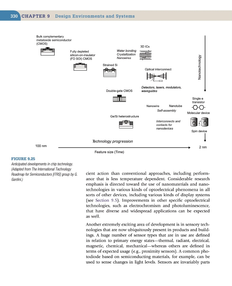
Figure 9.25
Anticipated developments in chip technology.
(Adapted from The International Technology
Roadmap for Semiconductors [ITRS] group by G.
Gardini.)
Technology progression
Nanotechnology
Bulk complementary
metatoxide semiconductor
(CMOS)
Ge/Si heterostructure
Fully depleted
silicon-on-insulator
(FD SOI) CMOS
Strained Si
3D ICs
Double-gate CMOS
Nanowire
Optical interconnect
Nanotube
Single e
transistor
Molecular device
Spin device
Detectors, lasers, modulators,
waveguides
Detectors, lasers, modulators,
waveguides
Interconnects and
contacts for
nanodevices
Water bonding
Crystallization
Nanowires
Self-assembly
=
B
Feature size (Time)
100 nm
2 nm
330
cient action than conventional approaches, including performance that is less temperature dependent. Considerable research
emphasis is directed toward the use of nanomaterials and nanotechnologies in various kinds of optoelectrical phenomena in all
sorts of other devices, including various kinds of display systems
(see Section 9.5). Improvements in other specific optoelectrical
technologies, such as electrochromism and photoluminescence,
that have diverse and widespread applications can be expected
as well.
Another extremely exciting area of development is in sensory technologies that are now ubiquitously present in products and buildings. A huge number of sensor types that are in use are defined
in relation to primary energy states—thermal, radiant, electrical,
magnetic, chemical, mechanical—whereas others are defined in
terms of expected usage (e.g., proximity sensors). A common photodiode based on semiconducting materials, for example, can be
used to sense changes in light levels. Sensors are invariably parts
Figure 9.25
Anticipated developments in chip technology.
(Adapted from The International Technology
Roadmap for Semiconductors [ITRS] group by G.
Gardini.)
Technology progression
Nanotechnology
Bulk complementary
metatoxide semiconductor
(CMOS)
Ge/Si heterostructure
Fully depleted
silicon-on-insulator
(FD SOI) CMOS
Strained Si
3D ICs
Double-gate CMOS
Nanowire
Optical interconnect
Nanotube
Single e
transistor
Molecular device
Spin device
Detectors, lasers, modulators,
waveguides
Detectors, lasers, modulators,
waveguides
Interconnects and
contacts for
nanodevices
Water bonding
Crystallization
Nanowires
Self-assembly
=
B
Feature size (Time)
100 nm
2 nm