

2.7 Classification of X-ray Detectors
69
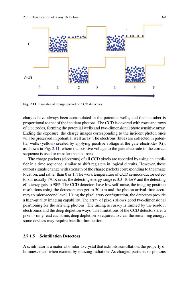
Fig. 2.11 Transfer of charge packet of CCD detectors
charges have always been accumulated in the potential wells, and their number is
proportional to that of the incident photons. The CCD is covered with rows and rows
of electrodes, forming the potential wells and two-dimensional photosensitive array.
Ending the exposure, the charge images corresponding to the incident photon ones
will be preserved in potential well array. The electrons (blue) are collected in potential wells (yellow) created by applying positive voltage at the gate electrodes (G),
as shown in Fig. 2.11, where the positive voltage to the gate electrode in the correct
sequence is used to transfer the electrons.
The charge packets (electrons) of all CCD pixels are recorded by using an amplifier in a time sequence, similar to shift registers in logical circuits. However, these
output signals change with strength of the charge packets corresponding to the image
location, and rather than 0 or 1. The work temperature of CCD semiconductor detectors is usually 170 K or so, the detecting energy range is 0.3–10 keV and the detecting
efficiency gets to 90%. The CCD detectors have low self-noise, the imaging position
resolutions using the detectors can get to 30 µm and the photon arrival-time accuracy to microsecond level. Using the pixel array configuration, the detectors provide
a high-quality imaging capability. The array of pixels allows good two-dimensional
positioning for the arriving photons. The timing accuracy is limited by the readout
electronics and the deep depletion ways. The limitations of the CCD detectors are: a
pixel is only read each time; deep depletion is required to clear the remaining energy;
some devices may require backlit illumination.
2.7.1.5 Scintillation Detectors
A scintillator is a material similar to crystal that exhibits scintillation, the property of
luminescence, when excited by ionizing radiation. As charged particles or photons
69
Fig. 2.11 Transfer of charge packet of CCD detectors
charges have always been accumulated in the potential wells, and their number is
proportional to that of the incident photons. The CCD is covered with rows and rows
of electrodes, forming the potential wells and two-dimensional photosensitive array.
Ending the exposure, the charge images corresponding to the incident photon ones
will be preserved in potential well array. The electrons (blue) are collected in potential wells (yellow) created by applying positive voltage at the gate electrodes (G),
as shown in Fig. 2.11, where the positive voltage to the gate electrode in the correct
sequence is used to transfer the electrons.
The charge packets (electrons) of all CCD pixels are recorded by using an amplifier in a time sequence, similar to shift registers in logical circuits. However, these
output signals change with strength of the charge packets corresponding to the image
location, and rather than 0 or 1. The work temperature of CCD semiconductor detectors is usually 170 K or so, the detecting energy range is 0.3–10 keV and the detecting
efficiency gets to 90%. The CCD detectors have low self-noise, the imaging position
resolutions using the detectors can get to 30 µm and the photon arrival-time accuracy to microsecond level. Using the pixel array configuration, the detectors provide
a high-quality imaging capability. The array of pixels allows good two-dimensional
positioning for the arriving photons. The timing accuracy is limited by the readout
electronics and the deep depletion ways. The limitations of the CCD detectors are: a
pixel is only read each time; deep depletion is required to clear the remaining energy;
some devices may require backlit illumination.
2.7.1.5 Scintillation Detectors
A scintillator is a material similar to crystal that exhibits scintillation, the property of
luminescence, when excited by ionizing radiation. As charged particles or photons