

3.3. MICROSCOPY
47
Coventional TEM
b
I
Obj
Lens
I
Lens
Scanning TEM
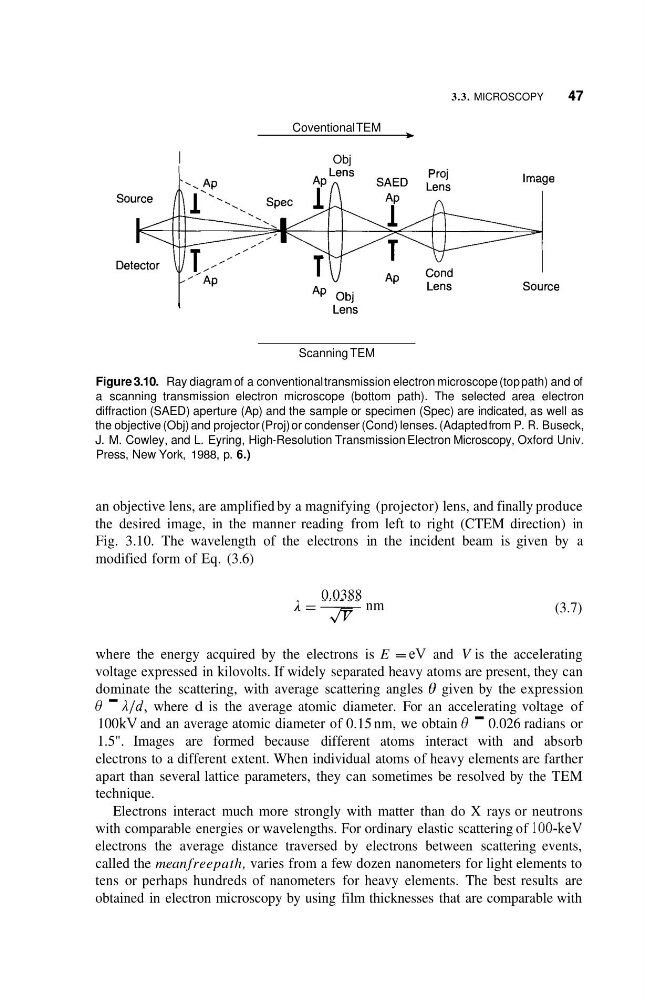
Figure 3.10. Ray diagram of a conventional transmission electron microscope (top path) and of
a scanning transmission electron microscope (bottom path). The selected area electron
diffraction (SAED) aperture (Ap) and the sample or specimen (Spec) are indicated, as well as
the objective (Obj) and projector (Proj) or condenser (Cond) lenses. (Adapted from P. R. Buseck,
J. M. Cowley, and L. Eyring, High-Resolution Transmission Electron Microscopy, Oxford Univ.
Press, New York, 1988, p. 6.)
an objective lens, are amplified by a magnifying (projector) lens, and finally produce
the desired image, in the manner reading from left to right (CTEM direction) in
Fig. 3.10. The wavelength of the electrons in the incident beam is given by a
modified form of Eq. (3.6)
0.0388
A=nm
f l
(3.7)
where the energy acquired by the electrons is E = eV and V is the accelerating
voltage expressed in kilovolts. If widely separated heavy atoms are present, they can
dominate the scattering, with average scattering angles Q given by the expression
0 - A/d, where d is the average atomic diameter. For an accelerating voltage of
100 kV and an average atomic diameter of 0.15 nm, we obtain 0 - 0.026 radians or
1.5". Images are formed because different atoms interact with and absorb
electrons to a different extent. When individual atoms of heavy elements are farther
apart than several lattice parameters, they can sometimes be resolved by the TEM
technique.
Electrons interact much more strongly with matter than do X rays or neutrons
with comparable energies or wavelengths. For ordinary elastic scattering of 100-keV
electrons the average distance traversed by electrons between scattering events,
called the mean freepath, varies from a few dozen nanometers for light elements to
tens or perhaps hundreds of nanometers for heavy elements. The best results are
obtained in electron microscopy by using film thicknesses that are comparable with
47
Coventional TEM
b
I
Obj
Lens
I
Lens
Scanning TEM
Figure 3.10. Ray diagram of a conventional transmission electron microscope (top path) and of
a scanning transmission electron microscope (bottom path). The selected area electron
diffraction (SAED) aperture (Ap) and the sample or specimen (Spec) are indicated, as well as
the objective (Obj) and projector (Proj) or condenser (Cond) lenses. (Adapted from P. R. Buseck,
J. M. Cowley, and L. Eyring, High-Resolution Transmission Electron Microscopy, Oxford Univ.
Press, New York, 1988, p. 6.)
an objective lens, are amplified by a magnifying (projector) lens, and finally produce
the desired image, in the manner reading from left to right (CTEM direction) in
Fig. 3.10. The wavelength of the electrons in the incident beam is given by a
modified form of Eq. (3.6)
0.0388
A=nm
f l
(3.7)
where the energy acquired by the electrons is E = eV and V is the accelerating
voltage expressed in kilovolts. If widely separated heavy atoms are present, they can
dominate the scattering, with average scattering angles Q given by the expression
0 - A/d, where d is the average atomic diameter. For an accelerating voltage of
100 kV and an average atomic diameter of 0.15 nm, we obtain 0 - 0.026 radians or
1.5". Images are formed because different atoms interact with and absorb
electrons to a different extent. When individual atoms of heavy elements are farther
apart than several lattice parameters, they can sometimes be resolved by the TEM
technique.
Electrons interact much more strongly with matter than do X rays or neutrons
with comparable energies or wavelengths. For ordinary elastic scattering of 100-keV
electrons the average distance traversed by electrons between scattering events,
called the mean freepath, varies from a few dozen nanometers for light elements to
tens or perhaps hundreds of nanometers for heavy elements. The best results are
obtained in electron microscopy by using film thicknesses that are comparable with