

40
METHODS OF MEASURING PROPERTIES
0 TEM histogram
_ _ _ _ Lognormal fit
0
5
10
15
20
Grain size (nm)
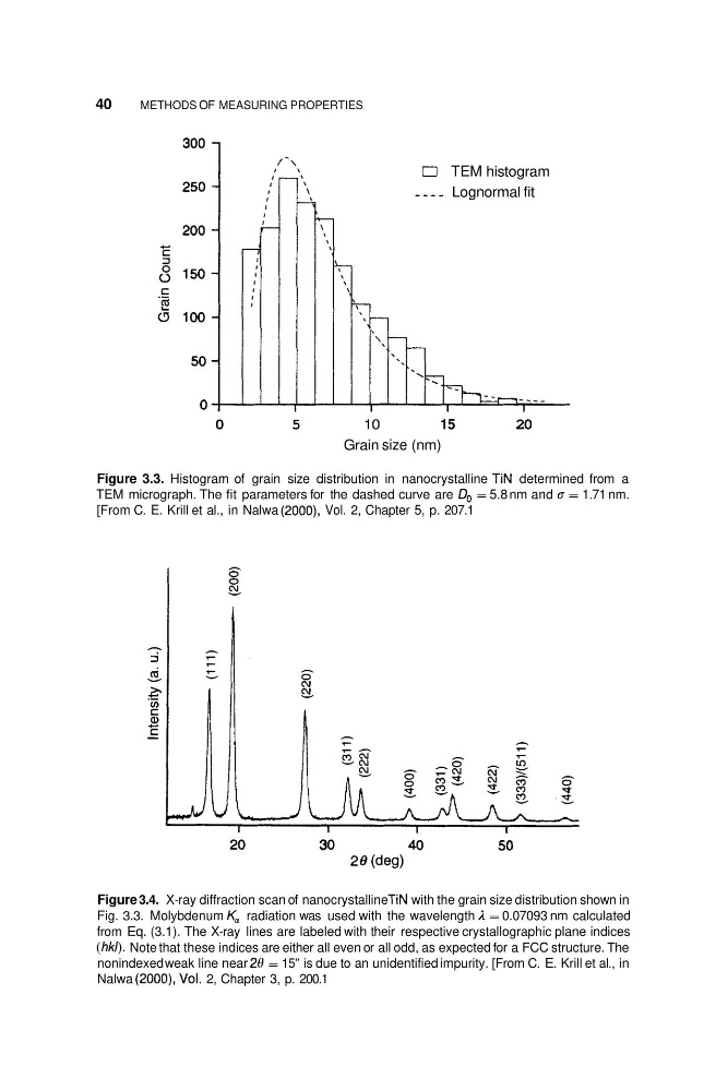
Figure 3.3. Histogram of grain size distribution in nanocrystalline TIN determined from a
TEM micrograph. The fit parameters for the dashed curve are 0, = 5.8 nm and CJ = 1.71 nm.
[From C. E. Krill et al., in Nalwa (2000), Vol. 2, Chapter 5, p. 207.1
Figure 3.4. X-ray diffraction scan of nanocrystalline TIN with the grain size distribution shown in
Fig. 3.3. Molybdenum K, radiation was used with the wavelength I = 0.07093 nm calculated
from Eq. (3.1). The X-ray lines are labeled with their respective crystallographic plane indices
(hkl). Note that these indices are either all even or all odd, as expected for a FCC structure. The
nonindexed weak line near 20 = 15” is due to an unidentified impurity. [From C. E. Krill et al., in
Nalwa (2000), Vol. 2, Chapter 3, p. 200.1
METHODS OF MEASURING PROPERTIES
0 TEM histogram
_ _ _ _ Lognormal fit
0
5
10
15
20
Grain size (nm)
Figure 3.3. Histogram of grain size distribution in nanocrystalline TIN determined from a
TEM micrograph. The fit parameters for the dashed curve are 0, = 5.8 nm and CJ = 1.71 nm.
[From C. E. Krill et al., in Nalwa (2000), Vol. 2, Chapter 5, p. 207.1
Figure 3.4. X-ray diffraction scan of nanocrystalline TIN with the grain size distribution shown in
Fig. 3.3. Molybdenum K, radiation was used with the wavelength I = 0.07093 nm calculated
from Eq. (3.1). The X-ray lines are labeled with their respective crystallographic plane indices
(hkl). Note that these indices are either all even or all odd, as expected for a FCC structure. The
nonindexed weak line near 20 = 15” is due to an unidentified impurity. [From C. E. Krill et al., in
Nalwa (2000), Vol. 2, Chapter 3, p. 200.1