

2.3. LOCALIZED PARTICLES
31
add electrons to the acceptors are much less than the thermal energy at room
temperature T = 300 K, that is, AED, AE, << k, T , so virtually all donors are positively ionized and virtually all acceptors are negatively ionized at room temperature.
The donor and acceptor atoms that we have been discussing are known as shallow
centers, that is, shallow traps of electrons or holes, because their excitation energies
are much less than that of the bandgap (AED, AEA << Eg). There are other centers
with energy levels that lie deep within the forbidden gap, often closer to its center
than to the top or bottom, in contrast to the case with shallow donors and acceptors.
Since generally Eg >> k,T, these traps are not extensively ionized, and the energies
involved in exciting or ionizing them are not small. Examples of deep centers are
defects associated with broken bonds, or strain involving displacements of atoms. In
Chapter 8 we discuss how deep centers can produce characteristic optical spectroscopic effects.
2.3.2. Mobility
Another important parameter of a semiconductor is the mobility p or charge carrier
drift velocity u per unit electric field E, given by the expression p = (ul/E. This
parameter is defined as positive for both electrons and holes. Table B.9 lists the
mobilities pe and p,, for electrons and holes, respectively, in the semiconductors
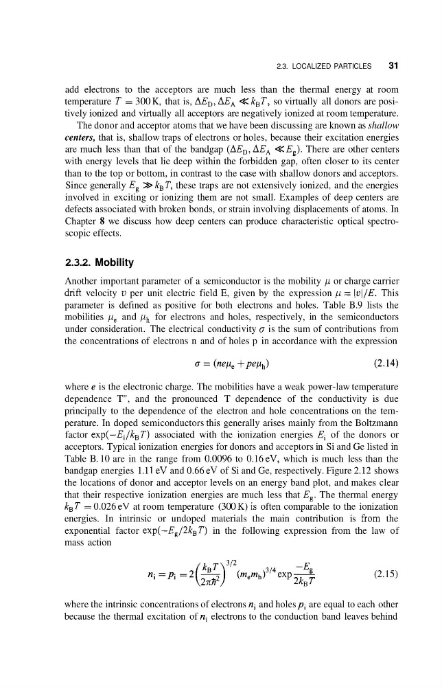
under consideration. The electrical conductivity (T is the sum of contributions from
the concentrations of electrons n and of holes p in accordance with the expression
where e is the electronic charge. The mobilities have a weak power-law temperature
dependence T", and the pronounced T dependence of the conductivity is due
principally to the dependence of the electron and hole concentrations on the temperature. In doped semiconductors this generally arises mainly from the Boltzmann
factor exp(-Ei/kBT) associated with the ionization energies Ei of the donors or
acceptors. Typical ionization energies for donors and acceptors in Si and Ge listed in
Table B. 10 are in the range from 0.0096 to 0.16 eV, which is much less than the
bandgap energies 1.1 1 eV and 0.66 eV of Si and Ge, respectively. Figure 2.12 shows
the locations of donor and acceptor levels on an energy band plot, and makes clear
that their respective ionization energies are much less that Eg. The thermal energy
kBT = 0.026 eV at room temperature (300 K) is often comparable to the ionization
energies. In intrinsic or undoped materials the main contribution is from the
exponential factor exp(-E,/2kBT) in the following expression from the law of
mass action
-EP
ni = p i = 2($)
(rnernh)3/4 exp312
2 k ~
T
(2.15)
where the intrinsic concentrations of electrons ni and holes pi are equal to each other
because the thermal excitation of ni electrons to the conduction band leaves behind
31
add electrons to the acceptors are much less than the thermal energy at room
temperature T = 300 K, that is, AED, AE, << k, T , so virtually all donors are positively ionized and virtually all acceptors are negatively ionized at room temperature.
The donor and acceptor atoms that we have been discussing are known as shallow
centers, that is, shallow traps of electrons or holes, because their excitation energies
are much less than that of the bandgap (AED, AEA << Eg). There are other centers
with energy levels that lie deep within the forbidden gap, often closer to its center
than to the top or bottom, in contrast to the case with shallow donors and acceptors.
Since generally Eg >> k,T, these traps are not extensively ionized, and the energies
involved in exciting or ionizing them are not small. Examples of deep centers are
defects associated with broken bonds, or strain involving displacements of atoms. In
Chapter 8 we discuss how deep centers can produce characteristic optical spectroscopic effects.
2.3.2. Mobility
Another important parameter of a semiconductor is the mobility p or charge carrier
drift velocity u per unit electric field E, given by the expression p = (ul/E. This
parameter is defined as positive for both electrons and holes. Table B.9 lists the
mobilities pe and p,, for electrons and holes, respectively, in the semiconductors
under consideration. The electrical conductivity (T is the sum of contributions from
the concentrations of electrons n and of holes p in accordance with the expression
where e is the electronic charge. The mobilities have a weak power-law temperature
dependence T", and the pronounced T dependence of the conductivity is due
principally to the dependence of the electron and hole concentrations on the temperature. In doped semiconductors this generally arises mainly from the Boltzmann
factor exp(-Ei/kBT) associated with the ionization energies Ei of the donors or
acceptors. Typical ionization energies for donors and acceptors in Si and Ge listed in
Table B. 10 are in the range from 0.0096 to 0.16 eV, which is much less than the
bandgap energies 1.1 1 eV and 0.66 eV of Si and Ge, respectively. Figure 2.12 shows
the locations of donor and acceptor levels on an energy band plot, and makes clear
that their respective ionization energies are much less that Eg. The thermal energy
kBT = 0.026 eV at room temperature (300 K) is often comparable to the ionization
energies. In intrinsic or undoped materials the main contribution is from the
exponential factor exp(-E,/2kBT) in the following expression from the law of
mass action
-EP
ni = p i = 2($)
(rnernh)3/4 exp312
2 k ~
T
(2.15)
where the intrinsic concentrations of electrons ni and holes pi are equal to each other
because the thermal excitation of ni electrons to the conduction band leaves behind