

2.2. ENERGY BANDS
29
bands of Figs. 2.15 and 2.18 that the actual dependence of the energy E on k is much
more complex than Eq. (2.9) indicates. Equation (2.1 1) provides a general definition
of the effective mass, designated by the symbol m*, and the wavevector k
dependence of m* can be evaluated from the band structure plots by carrying out
the differentiations. We see from a comparison of the slopes near the conduction
band minimum and the valence band maximum of GaAs at the point on Fig. 2.15
(see also Fig. 2.16) that the upper electron bands have steeper slopes and hence
lighter masses than do the lower hole bands with more gradual slopes.
2.2.5. Fermi Surfaces
At very low temperatures electrons fill the energy bands of solids up to an energy
called the Fermi energy EF, and the bands are empty for energies that exceed E F . In
three-dimensional k space the set of values of kx, ky, and k,, which satisfy the
equation A2(k: + k; + k,2)/2m = EF, form a surface called the Fermi surface. All
k,,k,,k, energy states that lie below this surface are full, and the states above the
surface are empty. The Fermi surface encloses all the electrons in the conduction
band that carry electric current. In the good conductors copper and silver the
conduction electron density is 8.5 x
and 5.86 x 10²²electrons/cm3, respectively. From another viewpoint, the Fermi surface of a good conductor can fill the
entire Brillouin zone. In the intrinsic semiconductors GaAs, Si, and Ge the carrier
density at room temperature from Fig. 2.17 is approximately lo6, lO' O, and
1 OI3 camers/cm3, respectively, many orders of magnitude below that of metals,
and semiconductors are seldom doped to concentrations above 1019 centers/cm3. An
intrinsic semiconductor is one with a full valence band and an empty conduction
band at absolute zero of temperature. As we saw above, at ambient temperatures
some electrons are thermally excited to the bottom of the conduction band, and an
equal number of empty sites or holes are left behind near the top of the valence band.
This means that only a small percentage of the Brillouin zone contains electrons in
the conduction band, and the number of holes in the valence band is correspondingly
small. In a one-dimensional representation this reflects the electron and hole
occupancies depicted in Fig. 2.16.
point in the center of the Brillouin
zone, as is the case with GaAs, then it will be very close to a sphere since the
symmetry is cubic, and to a good approximation we can assume a quadratic
dependence of the energy on the wavevector k, corresponding to Eq. (2.9). Therefore
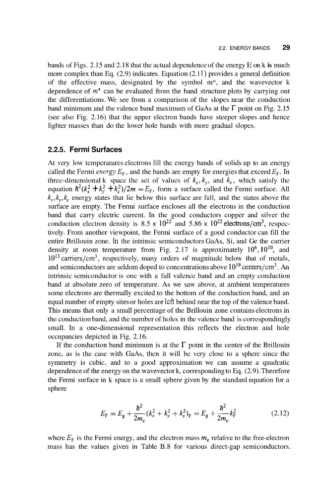
the Fermi surface in k space is a small sphere given by the standard equation for a
sphere
If the conduction band minimum is at the
(2.12)
where E F is the Fermi energy, and the electron mass me relative to the free-electron
mass has the values given in Table B.8 for various direct-gap semiconductors.
29
bands of Figs. 2.15 and 2.18 that the actual dependence of the energy E on k is much
more complex than Eq. (2.9) indicates. Equation (2.1 1) provides a general definition
of the effective mass, designated by the symbol m*, and the wavevector k
dependence of m* can be evaluated from the band structure plots by carrying out
the differentiations. We see from a comparison of the slopes near the conduction
band minimum and the valence band maximum of GaAs at the point on Fig. 2.15
(see also Fig. 2.16) that the upper electron bands have steeper slopes and hence
lighter masses than do the lower hole bands with more gradual slopes.
2.2.5. Fermi Surfaces
At very low temperatures electrons fill the energy bands of solids up to an energy
called the Fermi energy EF, and the bands are empty for energies that exceed E F . In
three-dimensional k space the set of values of kx, ky, and k,, which satisfy the
equation A2(k: + k; + k,2)/2m = EF, form a surface called the Fermi surface. All
k,,k,,k, energy states that lie below this surface are full, and the states above the
surface are empty. The Fermi surface encloses all the electrons in the conduction
band that carry electric current. In the good conductors copper and silver the
conduction electron density is 8.5 x
and 5.86 x 10²²electrons/cm3, respectively. From another viewpoint, the Fermi surface of a good conductor can fill the
entire Brillouin zone. In the intrinsic semiconductors GaAs, Si, and Ge the carrier
density at room temperature from Fig. 2.17 is approximately lo6, lO' O, and
1 OI3 camers/cm3, respectively, many orders of magnitude below that of metals,
and semiconductors are seldom doped to concentrations above 1019 centers/cm3. An
intrinsic semiconductor is one with a full valence band and an empty conduction
band at absolute zero of temperature. As we saw above, at ambient temperatures
some electrons are thermally excited to the bottom of the conduction band, and an
equal number of empty sites or holes are left behind near the top of the valence band.
This means that only a small percentage of the Brillouin zone contains electrons in
the conduction band, and the number of holes in the valence band is correspondingly
small. In a one-dimensional representation this reflects the electron and hole
occupancies depicted in Fig. 2.16.
point in the center of the Brillouin
zone, as is the case with GaAs, then it will be very close to a sphere since the
symmetry is cubic, and to a good approximation we can assume a quadratic
dependence of the energy on the wavevector k, corresponding to Eq. (2.9). Therefore
the Fermi surface in k space is a small sphere given by the standard equation for a
sphere
If the conduction band minimum is at the
(2.12)
where E F is the Fermi energy, and the electron mass me relative to the free-electron
mass has the values given in Table B.8 for various direct-gap semiconductors.