

146
BULK NANOSTRUCTURED MATERIALS
,
.
T=O
tE
y;:pEF2 . .
. .
. .
. .
. .
. .
. .
. .
. .
. .
. .
. .
T=O
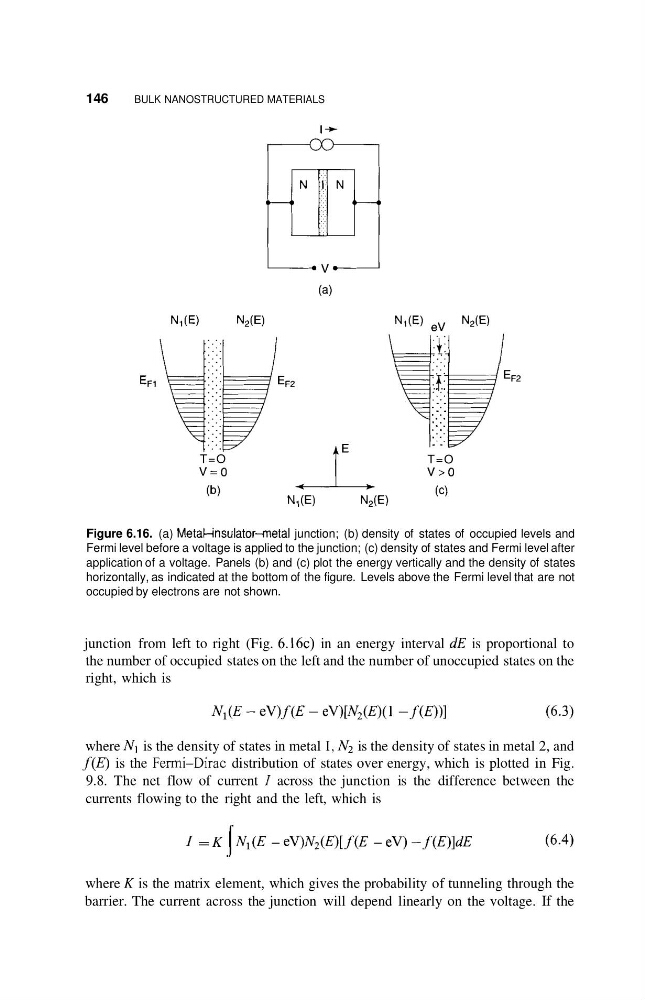
Figure 6.16. (a) Metal-insulator-metal junction; (b) density of states of occupied levels and
Fermi level before a voltage is applied to the junction; (c) density of states and Fermi level after
application of a voltage. Panels (b) and (c) plot the energy vertically and the density of states
horizontally, as indicated at the bottom of the figure. Levels above the Fermi level that are not
occupied by electrons are not shown.
junction from left to right (Fig. 6.16~) in an energy interval dE is proportional to
the number of occupied states on the left and the number of unoccupied states on the
right, which is
where N1 is the density of states in metal I , N2 is the density of states in metal 2, and
f(E) is the Fermi-Dirac distribution of states over energy, which is plotted in Fig.
9.8. The net flow of current I across the junction is the difference between the
currents flowing to the right and the left, which is
1 = K Nl(E - eV)N2(E)[f(E - eV) -f(E)]dE
(6.4)
. I .
where K is the matrix element, which gives the probability of tunneling through the
barrier. The current across the junction will depend linearly on the voltage. If the
BULK NANOSTRUCTURED MATERIALS
,
.
T=O
tE
y;:pEF2 . .
. .
. .
. .
. .
. .
. .
. .
. .
. .
. .
. .
T=O
Figure 6.16. (a) Metal-insulator-metal junction; (b) density of states of occupied levels and
Fermi level before a voltage is applied to the junction; (c) density of states and Fermi level after
application of a voltage. Panels (b) and (c) plot the energy vertically and the density of states
horizontally, as indicated at the bottom of the figure. Levels above the Fermi level that are not
occupied by electrons are not shown.
junction from left to right (Fig. 6.16~) in an energy interval dE is proportional to
the number of occupied states on the left and the number of unoccupied states on the
right, which is
where N1 is the density of states in metal I , N2 is the density of states in metal 2, and
f(E) is the Fermi-Dirac distribution of states over energy, which is plotted in Fig.
9.8. The net flow of current I across the junction is the difference between the
currents flowing to the right and the left, which is
1 = K Nl(E - eV)N2(E)[f(E - eV) -f(E)]dE
(6.4)
. I .
where K is the matrix element, which gives the probability of tunneling through the
barrier. The current across the junction will depend linearly on the voltage. If the