

86
3 SAMPA Chip Implementation
D
Q
D
Q
D
Q
Clock
Reset
Data in
Data out
(a) TMR protected register
D
Q
D
Q
D
Q
Clock
Reset
Data in
Data out
D
Q
D
Q
D
Q
(b) TMR protected synchronizer
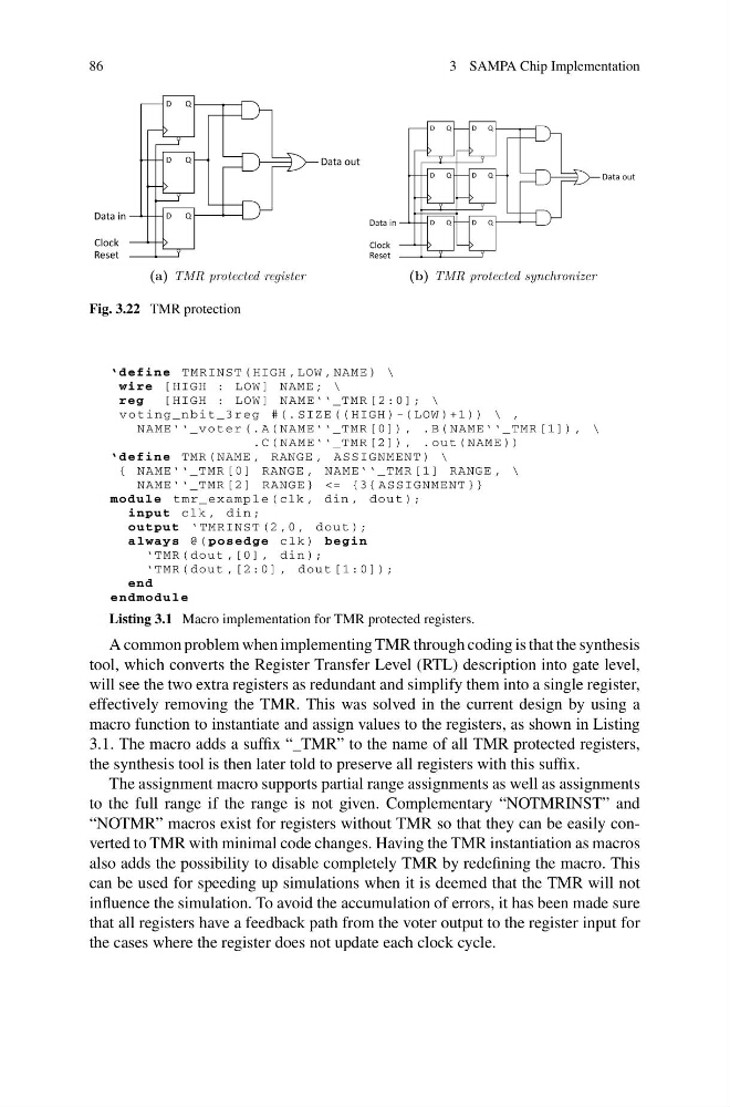
Fig. 3.22 TMR protection
‘define TMRINST ( HIGH , LOW , NAME ) \
wire [ HIGH : LOW ] NAME ; \
reg
[ HIGH : LOW ] NAME‘‘_TMR [2:0]; \
voting_nbit_3reg #(. SIZE (( HIGH ) -( LOW )+1)) \ ,
NAME‘‘_voter (. A ( NAME‘‘_TMR [0]) , . B ( NAME‘‘_TMR [1]) , \
. C ( NAME‘‘_TMR [2]) , . out ( NAME ))
‘define TMR ( NAME , RANGE , ASSIGNMENT ) \
{ NAME‘‘_TMR [0] RANGE , NAME‘‘_TMR [1] RANGE , \
NAME‘‘_TMR [2] RANGE } <= {3{ ASSIGNMENT }}
module tmr_example ( clk , din , dout );
input clk , din ;
output ‘TMRINST (2 ,0 , dout );
always @ ( posedge clk ) begin
‘TMR ( dout ,[0] , din );
‘TMR ( dout ,[2:0] , dout [1:0]);
end
endmodule
Listing 3.1 Macro implementation for TMR protected registers.
A common problem when implementing TMR through coding is that the synthesis
tool, which converts the Register Transfer Level (RTL) description into gate level,
will see the two extra registers as redundant and simplify them into a single register,
effectively removing the TMR. This was solved in the current design by using a
macro function to instantiate and assign values to the registers, as shown in Listing
3.1. The macro adds a suffix “_TMR” to the name of all TMR protected registers,
the synthesis tool is then later told to preserve all registers with this suffix.
The assignment macro supports partial range assignments as well as assignments
to the full range if the range is not given. Complementary “NOTMRINST” and
“NOTMR” macros exist for registers without TMR so that they can be easily converted to TMR with minimal code changes. Having the TMR instantiation as macros
also adds the possibility to disable completely TMR by redefining the macro. This
can be used for speeding up simulations when it is deemed that the TMR will not
influence the simulation. To avoid the accumulation of errors, it has been made sure
that all registers have a feedback path from the voter output to the register input for
the cases where the register does not update each clock cycle.
3 SAMPA Chip Implementation
D
Q
D
Q
D
Q
Clock
Reset
Data in
Data out
(a) TMR protected register
D
Q
D
Q
D
Q
Clock
Reset
Data in
Data out
D
Q
D
Q
D
Q
(b) TMR protected synchronizer
Fig. 3.22 TMR protection
‘define TMRINST ( HIGH , LOW , NAME ) \
wire [ HIGH : LOW ] NAME ; \
reg
[ HIGH : LOW ] NAME‘‘_TMR [2:0]; \
voting_nbit_3reg #(. SIZE (( HIGH ) -( LOW )+1)) \ ,
NAME‘‘_voter (. A ( NAME‘‘_TMR [0]) , . B ( NAME‘‘_TMR [1]) , \
. C ( NAME‘‘_TMR [2]) , . out ( NAME ))
‘define TMR ( NAME , RANGE , ASSIGNMENT ) \
{ NAME‘‘_TMR [0] RANGE , NAME‘‘_TMR [1] RANGE , \
NAME‘‘_TMR [2] RANGE } <= {3{ ASSIGNMENT }}
module tmr_example ( clk , din , dout );
input clk , din ;
output ‘TMRINST (2 ,0 , dout );
always @ ( posedge clk ) begin
‘TMR ( dout ,[0] , din );
‘TMR ( dout ,[2:0] , dout [1:0]);
end
endmodule
Listing 3.1 Macro implementation for TMR protected registers.
A common problem when implementing TMR through coding is that the synthesis
tool, which converts the Register Transfer Level (RTL) description into gate level,
will see the two extra registers as redundant and simplify them into a single register,
effectively removing the TMR. This was solved in the current design by using a
macro function to instantiate and assign values to the registers, as shown in Listing
3.1. The macro adds a suffix “_TMR” to the name of all TMR protected registers,
the synthesis tool is then later told to preserve all registers with this suffix.
The assignment macro supports partial range assignments as well as assignments
to the full range if the range is not given. Complementary “NOTMRINST” and
“NOTMR” macros exist for registers without TMR so that they can be easily converted to TMR with minimal code changes. Having the TMR instantiation as macros
also adds the possibility to disable completely TMR by redefining the macro. This
can be used for speeding up simulations when it is deemed that the TMR will not
influence the simulation. To avoid the accumulation of errors, it has been made sure
that all registers have a feedback path from the voter output to the register input for
the cases where the register does not update each clock cycle.