

122
5 Recent Advances in Zero-Index Photonics
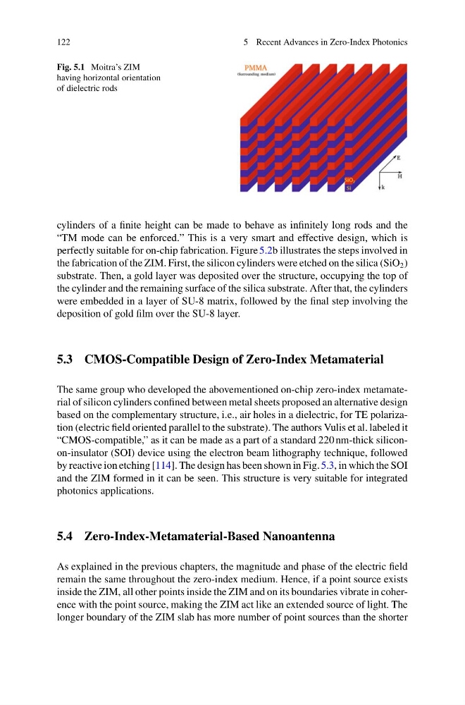
Fig. 5.1 Moitra’s ZIM
having horizontal orientation
of dielectric rods
cylinders of a finite height can be made to behave as infinitely long rods and the
“TM mode can be enforced.” This is a very smart and effective design, which is
perfectly suitable for on-chip fabrication. Figure 5.2b illustrates the steps involved in
the fabrication of the ZIM. First, the silicon cylinders were etched on the silica (SiO 2 )
substrate. Then, a gold layer was deposited over the structure, occupying the top of
the cylinder and the remaining surface of the silica substrate. After that, the cylinders
were embedded in a layer of SU-8 matrix, followed by the final step involving the
deposition of gold film over the SU-8 layer.
5.3 CMOS-Compatible Design of Zero-Index Metamaterial
The same group who developed the abovementioned on-chip zero-index metamaterial of silicon cylinders confined between metal sheets proposed an alternative design
based on the complementary structure, i.e., air holes in a dielectric, for TE polarization (electric field oriented parallel to the substrate). The authors Vulis et al. labeled it
“CMOS-compatible,” as it can be made as a part of a standard 220 nm-thick siliconon-insulator (SOI) device using the electron beam lithography technique, followed
by reactive ion etching [114]. The design has been shown in Fig. 5.3, in which the SOI
and the ZIM formed in it can be seen. This structure is very suitable for integrated
photonics applications.
5.4 Zero-Index-Metamaterial-Based Nanoantenna
As explained in the previous chapters, the magnitude and phase of the electric field
remain the same throughout the zero-index medium. Hence, if a point source exists
inside the ZIM, all other points inside the ZIM and on its boundaries vibrate in coherence with the point source, making the ZIM act like an extended source of light. The
longer boundary of the ZIM slab has more number of point sources than the shorter
5 Recent Advances in Zero-Index Photonics
Fig. 5.1 Moitra’s ZIM
having horizontal orientation
of dielectric rods
cylinders of a finite height can be made to behave as infinitely long rods and the
“TM mode can be enforced.” This is a very smart and effective design, which is
perfectly suitable for on-chip fabrication. Figure 5.2b illustrates the steps involved in
the fabrication of the ZIM. First, the silicon cylinders were etched on the silica (SiO 2 )
substrate. Then, a gold layer was deposited over the structure, occupying the top of
the cylinder and the remaining surface of the silica substrate. After that, the cylinders
were embedded in a layer of SU-8 matrix, followed by the final step involving the
deposition of gold film over the SU-8 layer.
5.3 CMOS-Compatible Design of Zero-Index Metamaterial
The same group who developed the abovementioned on-chip zero-index metamaterial of silicon cylinders confined between metal sheets proposed an alternative design
based on the complementary structure, i.e., air holes in a dielectric, for TE polarization (electric field oriented parallel to the substrate). The authors Vulis et al. labeled it
“CMOS-compatible,” as it can be made as a part of a standard 220 nm-thick siliconon-insulator (SOI) device using the electron beam lithography technique, followed
by reactive ion etching [114]. The design has been shown in Fig. 5.3, in which the SOI
and the ZIM formed in it can be seen. This structure is very suitable for integrated
photonics applications.
5.4 Zero-Index-Metamaterial-Based Nanoantenna
As explained in the previous chapters, the magnitude and phase of the electric field
remain the same throughout the zero-index medium. Hence, if a point source exists
inside the ZIM, all other points inside the ZIM and on its boundaries vibrate in coherence with the point source, making the ZIM act like an extended source of light. The
longer boundary of the ZIM slab has more number of point sources than the shorter